Method to grow pure nanocrystalline diamond films at low temperatures and high deposition rates

a technology of pure nanocrystalline diamond and low temperature, which is applied in the direction of coating, transportation and packaging, layered products, etc., can solve the problem that the film is intrinsically inferior to the uncd film, and achieve the effect of high deposition rate and enhanced chemical vapor deposition

Active Publication Date: 2005-02-10
UCHICAGO ARGONNE LLC
View PDF11 Cites 43 Cited by
  • Summary
  • Abstract
  • Description
  • Claims
  • Application Information

AI Technical Summary

Benefits of technology

[0003] This invention relates to an improved method for preparing nanocrystalline diamond films. More specifically this invention relates to an improved method for preparing phase-pure nanocrystalline diamond films at low temperatures and with high deposition rates. Ultrananocrystalline diamond (UNCD) films grown at high temperatures (700-900° C.) have grain sizes between about 3 and about 5 nanometers and preferably are fully dense and continuous throughout. A method of preparing UNCD films is disclosed in U.S. patent application Ser. No. 10 / 845,867 filed May 13, 2004, the disclosure of which is incorporated herein by reference. Major techniques for depositing diamond-like films onto substrates involve using hydrogen-rich plasma chemistries via plasma enhanced chemical vapor deposition (PECVD) using either RF or microwave frequencies, and hot-filament reactors. The drawback to these techniques is that the deposition takes place at temperatures typically between 700° C. and 900° C. There are applications for diamond films in microelectromechanical systems (MEMS) and field emission, where the different materials in use require that the films be deposited at much lower temperatures, thus ruling out the use of materials that must be deposited at high temperatures. For example, many MEMS devices are fabricated on top of or co-planer with CMOS integrated circuit (IC) electronics. The “thermal budget” requirement for most IC chips, that is, the maximum duration at which the chip can be subjected to a given temperature, places not only a temperature constraint but also a time constraint on the deposition of the diamond film. For most CMOS chips this thermal budget is on the order of one hour (or less) for temperatures of about 350-450° C. Diamond-like carbon (DLC) films can be deposited at or near room temperature, but these films are intrinsically inferior to UNCD film.

Problems solved by technology

The drawback to these techniques is that the deposition takes place at temperatures typically between 700° C. and 900° C. There are applications for diamond films in microelectromechanical systems (MEMS) and field emission, where the different materials in use require that the films be deposited at much lower temperatures, thus ruling out the use of materials that must be deposited at high temperatures.
For most CMOS chips this thermal budget is on the order of one hour (or less) for temperatures of about 350-450° C. Diamond-like carbon (DLC) films can be deposited at or near room temperature, but these films are intrinsically inferior to UNCD film.

Method used


Image

  • Method to grow pure nanocrystalline diamond films at low temperatures and high deposition rates
  • Method to grow pure nanocrystalline diamond films at low temperatures and high deposition rates
  • Method to grow pure nanocrystalline diamond films at low temperatures and high deposition rates

Examples


Embodiment Construction

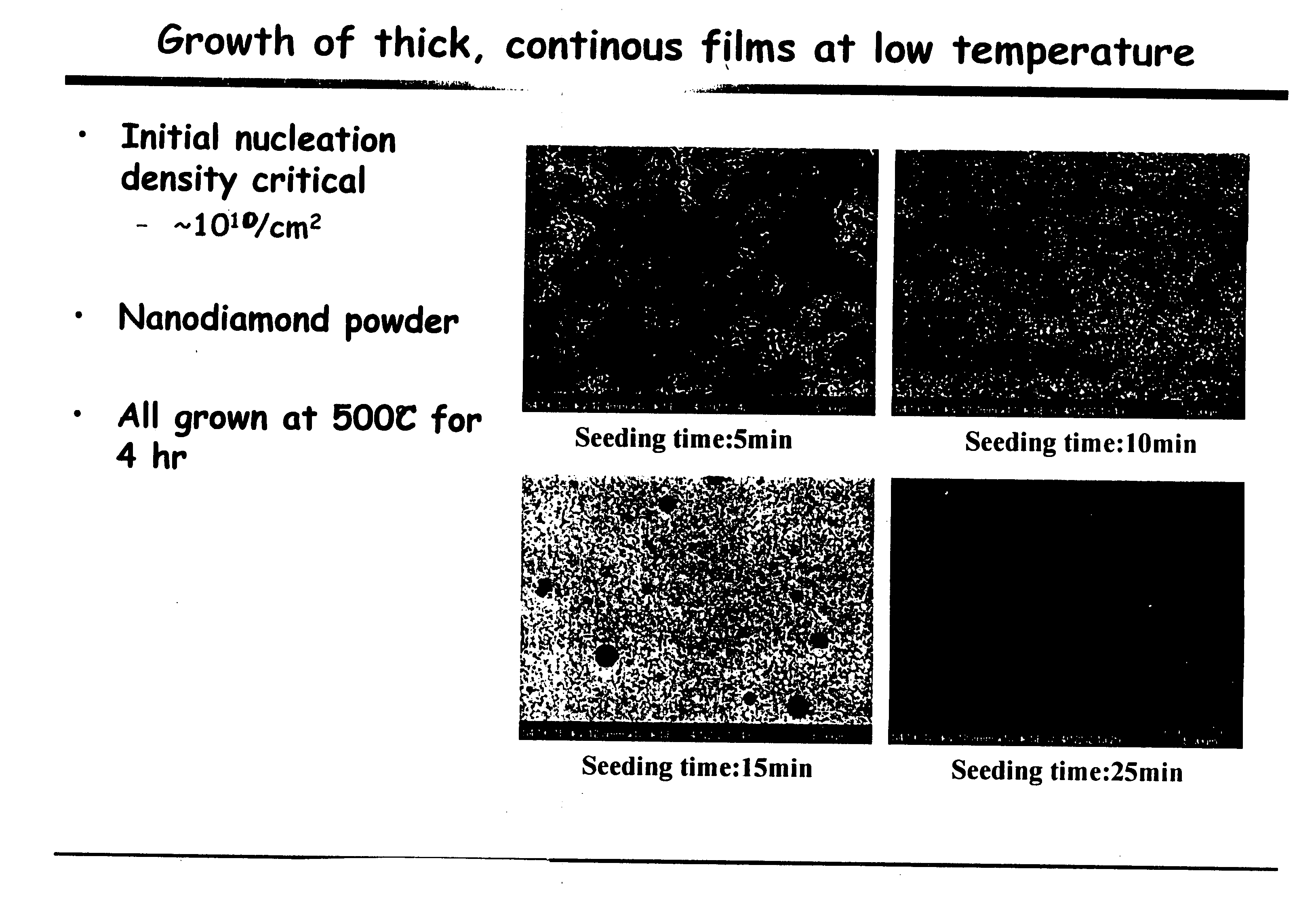
[0016] 1. A silicon wafer 100 mm in diameter was cleaned and seeded by immersing the wafer in an ultrasonic bath containing a mixture of nanometer sized diamond powder and an organic solvent (acetone, methanol, etc.). After the ultrasound, the wafer was removed from the bath and rinsed using a combination of organic solvent and distilled wafer. The seeding process was optimized to give the maximum initial areal nucleation density possible, about 1010 sites / cm2 (FIG. 1); however, nucleation areal densities in the range of from about 1010 to 1012 are satisfactory.

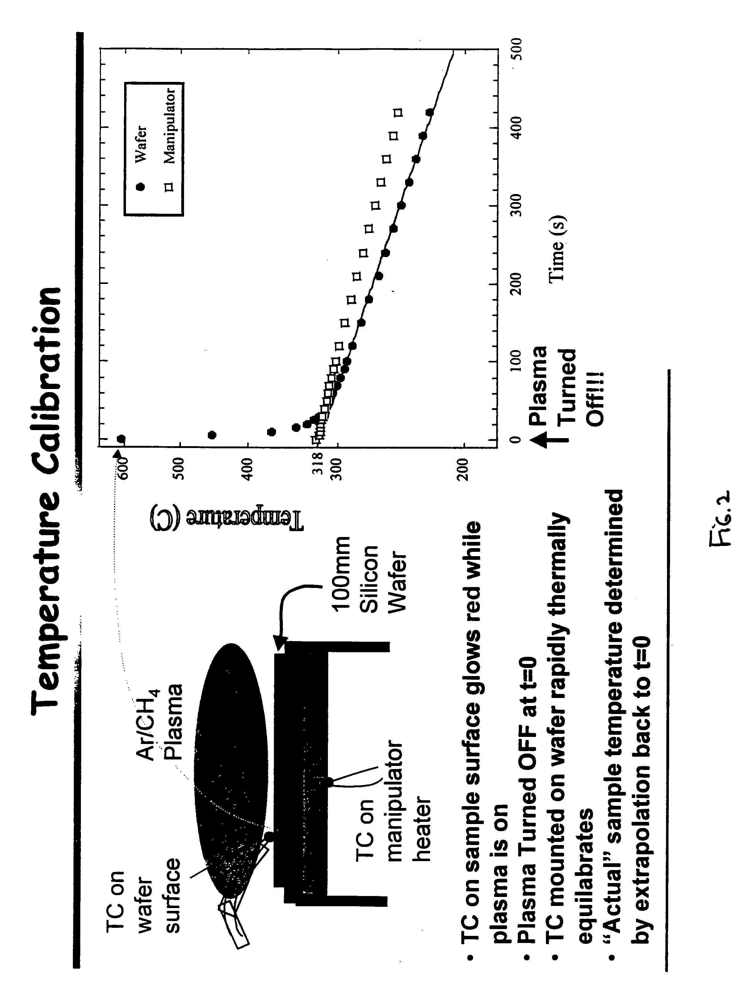
[0017] 2. Prior to UNCD deposition, the temperature of the substrate wafer during growth was calibrated through the use of a thermocouple mounted to the surface of a test wafer which was loaded into the microwave plasma chemical vapor deposition system and exposed to the same set of process conditions as would be used to grow a film at low temperatures (FIG. 2). It is not necessary to perform this step every time a low-tempe...


PUM

PropertyMeasurementUnit
temperatureaaaaaaaaaa
particle sizeaaaaaaaaaa

Abstract

A method of depositing nanocrystalline diamond film on a substrate at a rate of not less than about 0.2 microns/hour at a substrate temperature less than about 500° C. The method includes seeding the substrate surface with nanocrystalline diamond powder to an areal density of not less than about 1010sites/cm2, and contacting the seeded substrate surface with a gas of about 99% by volume of an inert gas other than helium and about 1% by volume of methane or hydrogen and one or more of acetylene, fullerene and anthracene in the presence of a microwave induced plasma while maintaining the substrate temperature less than about 500° C. to deposit nanocrystalline diamond on the seeded substrate surface at a rate not less than about 0.2 microns/hour. Coatings of nanocrystalline diamond with average particle diameters of less than about 20 nanometers can be deposited with thermal budgets of 500° C.-4 hours or less onto a variety of substrates such as MEMS devices.

Description

RELATED APPLICATIONS [0001] This application, pursuant to 37 C.F.R. 1.78(c), claims priority based on provisional application Ser. No. 60 / 493,152 filed on Aug. 7, 2003.[0002] The United States Government has rights in this invention pursuant to Contract No. W-31-109-ENG-38 between the U.S. Department of Energy (DOE) and The University of Chicago representing Argonne National Laboratory.SUMMARY OF THE INVENTION [0003] This invention relates to an improved method for preparing nanocrystalline diamond films. More specifically this invention relates to an improved method for preparing phase-pure nanocrystalline diamond films at low temperatures and with high deposition rates. Ultrananocrystalline diamond (UNCD) films grown at high temperatures (700-900° C.) have grain sizes between about 3 and about 5 nanometers and preferably are fully dense and continuous throughout. A method of preparing UNCD films is disclosed in U.S. patent application Ser. No. 10 / 845,867 filed May 13, 2004, the di...

Claims


Application Information

Patent Timeline
Patent Type & Authority Applications(United States)
IPC IPC(8): C23C16/27
CPCC23C16/274Y10T428/30C23C16/277
Inventor CARLISLE, JOHN A.GRUEN, DIETER M.AUCIELLO, ORLANDOXIAO, XINGCHENG
Owner UCHICAGO ARGONNE LLC
Why Eureka
Try Eureka