

EPIR device and semiconductor devices utilizing the same
a technology of epir and semiconductor, applied in the direction of instruments, nanoinformatics, substrate/intermediate layer, etc., can solve problems that cannot be considered to be necessarily realistic, and achieve the effects of improving epir characteristics, high practical utility, and excellent mass productivity
- Summary
- Abstract
- Description
- Claims
- Application Information
AI Technical Summary
Benefits of technology
Problems solved by technology
Method used
Image

Examples
embodiment 1
<Embodiment 1>
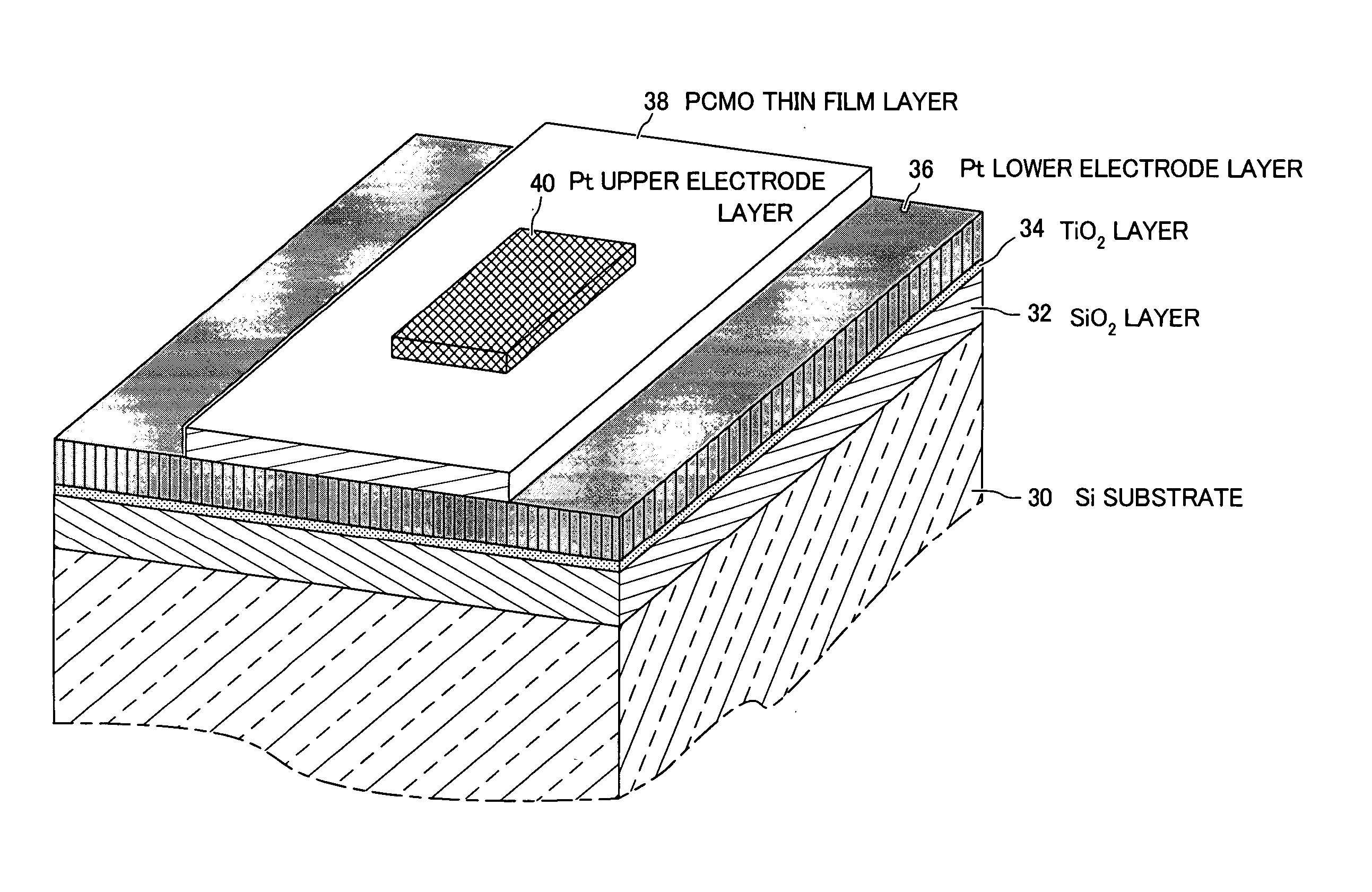
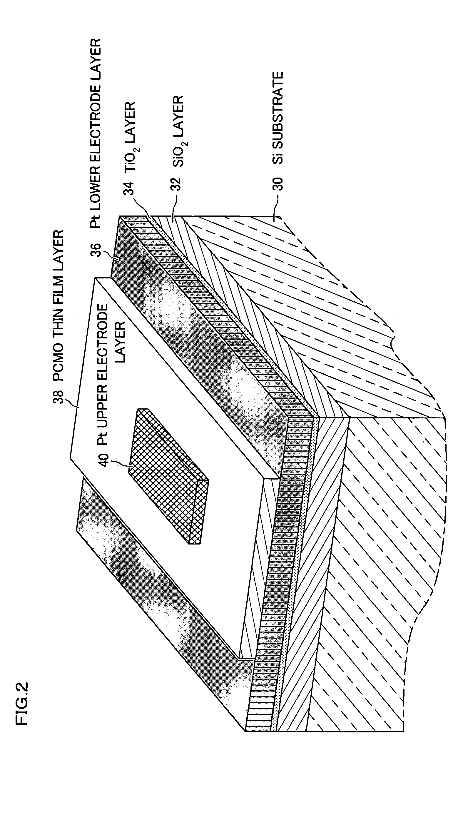
Firstly, Embodiment 1 of the present invention will be described with reference to the drawings. This embodiment is one relating to an EPIR device. FIG. 2 shows its multilayered structure. In FIG. 2, an Si substrate 30 having an SiO2 layer of 100 nm thick formed on its principal surface is prepared as a supporting or base substrate. Then, a TiO2 layer 34 is formed as a barrier adhesion layer on the SiO2 layer 32 of the Si substrate 30 by the reactive sputtering process.
Next, the Si substrate 30 which has been formed with the SiO2 layer 32 and the TiO2 layer 34 in this way, is heated to 400° C. and a Pt lower electrode layer 36 is formed as a noble metal electrode of 250 nm thick by the sputtering process using 100% Ar.
This Pt lower electrode layer 36 has been observed with an XRD (X-ray diffractometer) and a sectional TEM (transmission electron microscope) and it has been confirmed that it is mainly composed of columnar crystal grains of about 200 nm in grain...
embodiment 2
<Embodiment 2>
Next, Embodiment 2 of the present invention will be described. After a polycrystal Pt lower electrode layer 36 of the (1 1 1) orientation has been formed, a (Pr0.7Ca0.3) MnO3 thin film layer (PCMO thin film layer) is locally grown epitaxially to a film thickness of about 5 nm by the laser abrasion process using an O2 atmosphere of 20 mTorr and a substrate temperature of 600° C. at a low growth rate with a film forming rate of 2 nm / min.
It has been confirmed by the TEM observation that the (1 1 0)p plane which is most excellent in lattice matching with the Pt (1 1 1) crystal face and low in boundary energy is preferentially grown at such low growth rate. Also, the crystal orientation of the PCMO layer which is to be formed then consecutively is primarily determined by the orientation properties of the initially grown layer due to the extremely large contribution of the boundary energy even if the deposition rate is varied somewhat. Thus, if the layer is grown to ...
embodiment 3
<Embodiment 3>
Embodiment 3 of the present invention will now be described with reference to FIGS. 8 and 9. FIG. 8 shows the multilayer structure of an EPIR device according to the present embodiment. In the present embodiment, a low resistance Si substrate 60 subjected to a high-density impurity doping is used as a base substrate.
A TiN layer 62 is first formed on the principal surface of the Si substrate 60 by the reactive sputtering process. This TiN layer 62 is provided so as to not only provide an electric contact between a lower electrode layer and the Si substrate 60 of the EPIR device but also prevent any reaction between the material of the lower electrode layer and the material of the Si substrate 60. Then, the Si substrate 60 formed with this TiN layer 62 is heated to 400° C. and the Pt lower electrode layer 64 of 250 nm thick is formed by the sputtering process using 100% Ar. It has been confirmed that this Pt lower electrode layer 64 has the (1 1 1)-oriented polyc...
PUM
| Property | Measurement | Unit |
|---|---|---|
| magnetic field | aaaaa | aaaaa |
| thick | aaaaa | aaaaa |
| grain size | aaaaa | aaaaa |
Abstract
Description
Claims
Application Information