
Method and apparatus for article inspection including speckle reduction

a technology of article inspection and speckle reduction, which is applied in the field of inspection of articles, can solve the problems of reducing the yield of the fabrication line, false alarms, and insufficient brightness, and achieves the effects of reducing or eliminating speckle, reducing or eliminating the cost of being convenient in introducing large optical path length variations

Inactive Publication Date: 2005-06-16
APPLIED MATERIALS INC
View PDF99 Cites 27 Cited by
  • Summary
  • Abstract
  • Description
  • Claims
  • Application Information

AI Technical Summary

Benefits of technology

[0021] Another feature of the present invention resides in the provision of an optical system for reducing speckle in inspection systems operating at low wavelengths, particularly in the deep UV region.
[0033] Yet another embodiment of the present invention is constituted by an electro or acousto-optic modulator disposed along the light path and having an input surface for receiving the light beam and an output surface for transmitting an incoherent modulated beam to the area to be inspected. The high frequency bandwidth at which the modulator operates will alter randomly the optical wavefront phase of the input beam sufficiently to reduce or eliminate speckle. This embodiment has something of a disadvantage as compared with the previous embodiments because, for the shorter wavelengths such as deep UV, -optical modulators are relatively expensive. Since this solution works very well for sources with long coherence lengths, it may be used in combination with a fiber bundle or a grating, which work well at reducing speckle from sources with small and medium coherence lengths.

Problems solved by technology

Thus, any defect on the reticle would drastically reduce the yield of the fabrication line.
This is due to the fact that the physical resolution limit depends linearly on the illumination wavelength and due to interference effects which require that the inspection be done at a wavelength similar to the one used in the lithographic process.
As the wavelengths get smaller, conventional incoherent light sources like filament lamps or gas discharge lamps do not have enough brightness, and the light sources of choice become short wavelength lasers.
Speckle causes problems in detection of the surfaces of articles being inspected and causes false alarms because of the non uniformity of the light pattern hitting the detector.
The problem is an acute one in this type of article inspection, because the power provided by coherent light is essential, among other reasons, as a result of losses stemming from the detection process.
In such systems, speckle can have an adverse impact on yield and performance of the resulting devices, and so also must be addressed with great care.
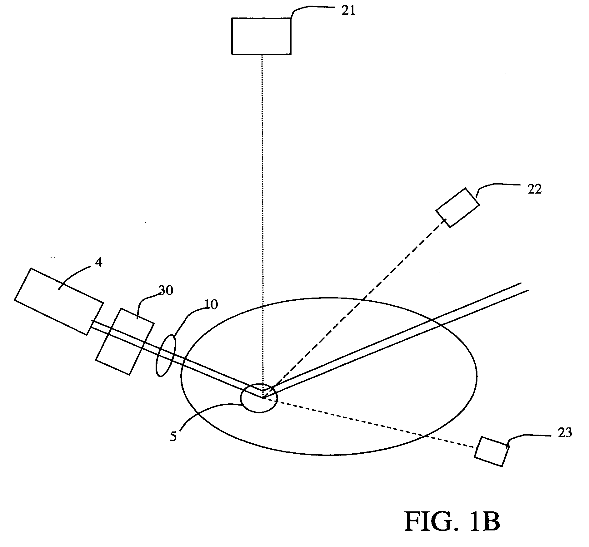
However, in some circumstances, such as oblique illumination (in which the coherent light source is directed to the wafer at an angle), the spot size will be sufficiently large to cause speckle.
With respect to the time integration methods, involving scanning of various planes of the imaging system and generating uncorrelated image patterns to be integrated by an image detector, the article identifies some possible drawbacks, such as a long integration time, or introduction of additional optical systems to support the scanning process.
However, as the reticles become smaller in size and the patterns shrink, it becomes more difficult to manufacture them with no fine anomalies and small defects.
With diffraction effects, the detection becomes more complicated as well.
Therefore, the danger exists that small defects may go undetected, which could cause problems in the related wafer manufacturing process.
None of the methods and systems discussed above is equipped to offer a high level of speckle reduction for low wavelength laser beams so as to ensure accurate defect detection.
Also, the above methods and systems do not provide a reliable solution for short laser pulses because of inadequate moving speed of the dispersing elements.
However, as with other known and proposed speckle reduction techniques, these proposed solutions do not address particular problems resulting from the need to work with extremely small features, and the consequent need to employ coherent illumination sources with very low wavelengths.
Speckle reduction devices, interposed in the light path between the article surface and the detector, also can be expensive.
These fiber bundles would be extremely large in size, and consequently would be expensive.
A similar problem would pertain with respect to the use of a diffraction grating.
The finer and larger in size the grating, the more expensive it would be.

Method used


Image

  • Method and apparatus for article inspection including speckle reduction
  • Method and apparatus for article inspection including speckle reduction
  • Method and apparatus for article inspection including speckle reduction

Examples


first embodiment

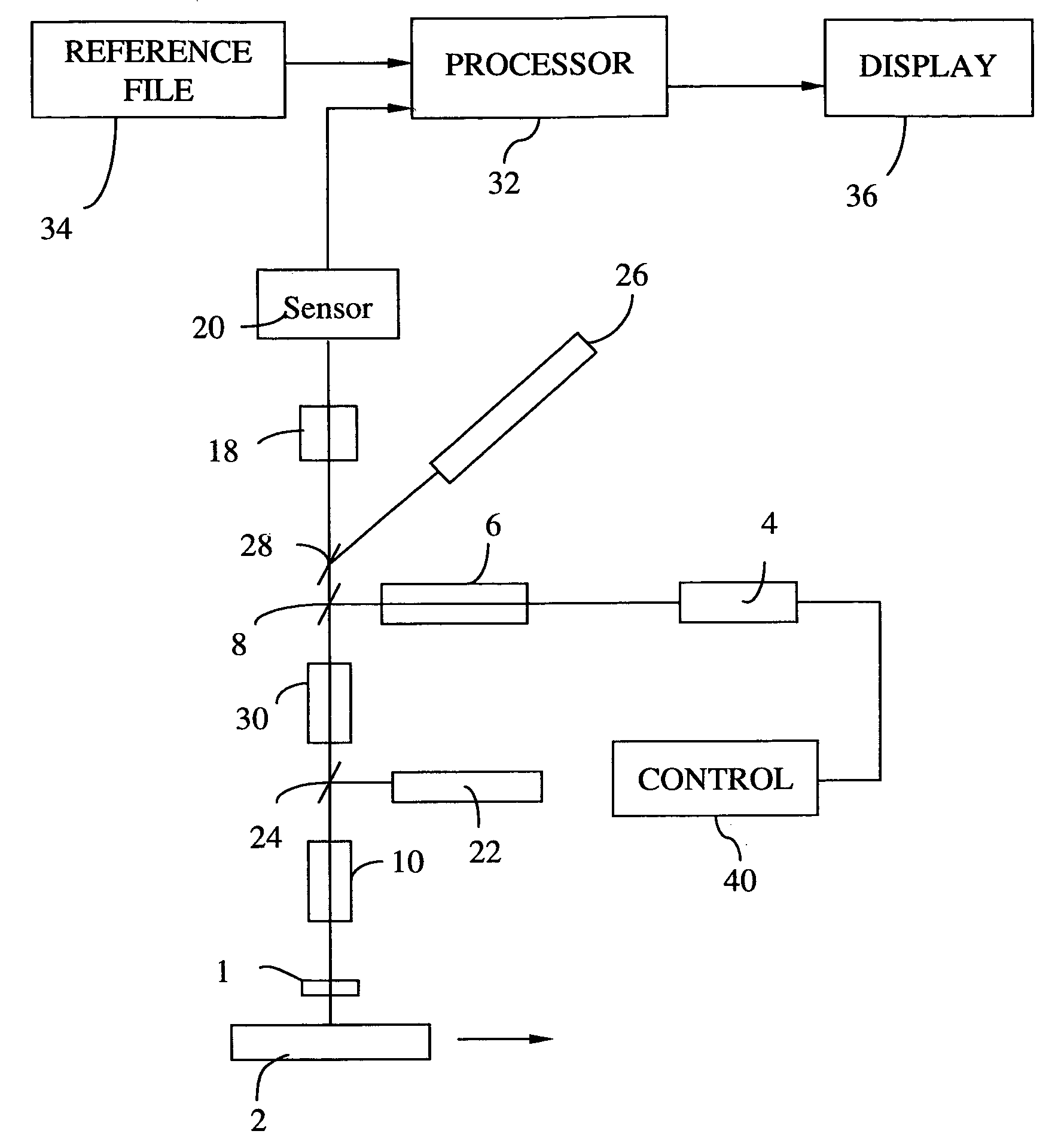
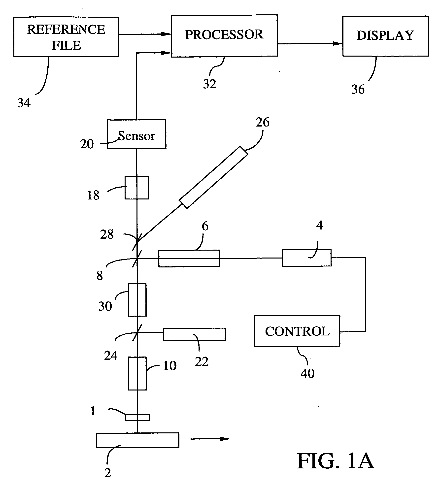
[0054] According to FIG. 2A, the coherence reduction optical apparatus 30 includes two optical fiber bundles 301 and 302, each having a predetermined number of optical fibers 304, 305. The bundles may have the same number of fibers, or different numbers of fibers. There also may be more than two bundles provided. The optical bundles 301 and 302 are sequentially positioned along the path of the imaging beam I, bundle 301 being positioned ahead of bundle 302 and having an input for receiving the imaging beam I and an output adjacent to an input of the second bundle 302. (For ease of description, the two bundles 301, 302 are shown at a slight angle with respect to each other, though in operation they may be aligned along an axis.).

[0055] The optical fibers 304 and 305 are of a similar type known in the art, preferably having predetermined parameters, such as refractive index and cladding, although they could also have different refractive indices or different claddings. The fibers 304 ...

second embodiment

[0064] In the present invention shown in FIG. 5, the coherence reduction optical apparatus 30 is constituted by an integrating sphere 311 disposed along the path of the imaging beam I. The integrating sphere 311 includes an entrance aperture 312 and an exit aperture 313. The aperture 312 has preferably a smaller diameter than the aperture 313. The aperture 312 is positioned so as to receive the imaging beam I. The integrating sphere 311 includes a non-absorbing inner surface made out of a non-absorbing material, preferably magnesium oxide (MgO), for better reflecting the imaging beam I. Other suitable reflective coatings also may be used.

[0065] After the imaging beam I is reflected within the integrating sphere 311, a reflected beam exits the sphere through the aperture 313. More specifically, the beam exiting the aperture 313 is a collection of reflected beams inside the integration sphere, each beam travelling a different distance from other beams. As a result, the collection of t...

third embodiment

[0069] As shown in FIG. 7, the coherence reduction optical apparatus 30 of present invention is constituted by a first grating 321 and a second grating 322, positioned along the path of the imaging beam I. The gratings 321, 322 in the embodiment are diffraction gratings, but it is to be understood that reflection gratings could be used with the same results. The gratings 321, 322 are preferably identical, having predetermined pitch A, wavelength λ, and first diffraction order, although gratings with different pitches and other properties could be used as well.

[0070] In operation, the imaging beam I hits the surface of grating 321 at a predetermined angle θi, and is diffracted at an angle θo. If the imaging beam I could be expanded to have a diameter D, as seen in FIG. 7, then an optical path difference (OPD) achieved between the two edges of the imaging beam can be calculated with the formula: OPD=Dtanθi+Dsinθo / cosθi; The diffraction relation is sinθo=λ / Λ−cosθi. The diffracted light...


PUM

PropertyMeasurementUnit
optical coherence lengthaaaaaaaaaa
lengthaaaaaaaaaa
lengthaaaaaaaaaa

Abstract

A method and apparatus for reducing speckle during inspection of articles used in the manufacture of semiconductor devices, including wafers, masks, photomasks, and reticles. The coherence of a light beam output by a coherent light source, such as a pulsed laser, is reduced by disposing elements in a light path. Examples of such elements include optical fiber bundles; optical light guides; optical gratings; an integrating sphere; and an acousto-optic modulator. These various elements may be combined as desired, such that light beams output by the element combinations have optical path length differences that are greater than a coherence length of the light beam output by the coherent light source.

Description

BACKGROUND OF THE INVENTION [0001] 1. Field of the Invention [0002] The present invention relates to inspection of articles, and in particular, to inspection of articles related to the manufacture of semiconductor devices. More specifically, the invention relates to the inspection of articles used in photolithography during the manufacture of semiconductor devices. [0003] 2. Description of the Related Art [0004] Current demands for high density and performance associated with ultra large scale integration in semiconductor devices require submicron features, increased transistor and circuit speeds, and improved reliability. Such demands require formation of device features with high precision and uniformity, which in turn necessitates careful process monitoring. [0005] One important process requiring careful inspection is photolithography, wherein masks or “reticles” are used to transfer circuitry patterns to semiconductor wafers. Typically, the reticles are in the form of patterned ...

Claims


Application Information

Patent Timeline
Patent Type & Authority Applications(United States)
IPC IPC(8): G01N21/47G01B11/30G01N21/95G01N21/956G02B27/48G03F1/00G03F7/20H01L21/027H01L21/66
CPCG01N21/4788G01N21/9501G01N21/956G03F7/70616G02B27/48G03F1/0092G01N2021/479G03F1/84
Inventor KARPOL, AVNERREINHORN, SILVIUELYSAF, EMANUELYALOV, SHIMONKENAN, BOAZ
Owner APPLIED MATERIALS INC
Learn More