Electronic circuit

Inactive Publication Date: 2005-07-07
SEMICON ENERGY LAB CO LTD
View PDF57 Cites 18 Cited by
  • Summary
  • Abstract
  • Description
  • Claims
  • Application Information

AI Technical Summary

Benefits of technology

[0005] It is an object of the present invention to provide a reliable electronic circuit having a semiconductor layer, conductive interconnects, and good

Problems solved by technology

Where electrodes should be formed on such a thin semiconductor layer, or an active layer, it has not been possible to make good contacts by the prior art techniques, because the thickness of the silicide layer grows almost up to the thickness of the semiconductor layer, thus severely deteriorating the electrical characteristics of

Method used


Image

  • Electronic circuit
  • Electronic circuit
  • Electronic circuit

Examples


example 1

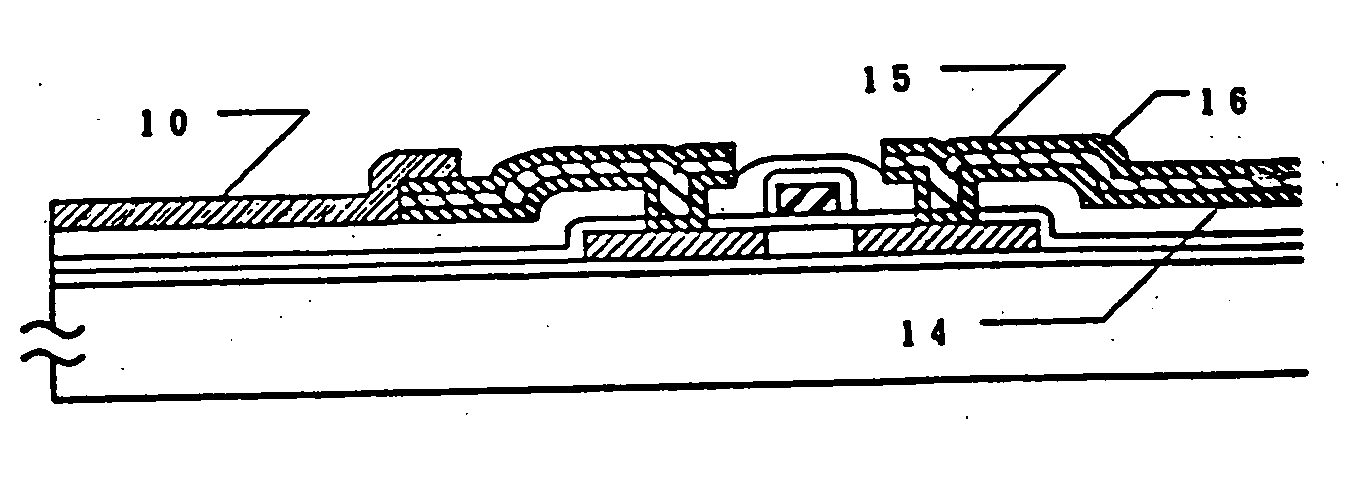
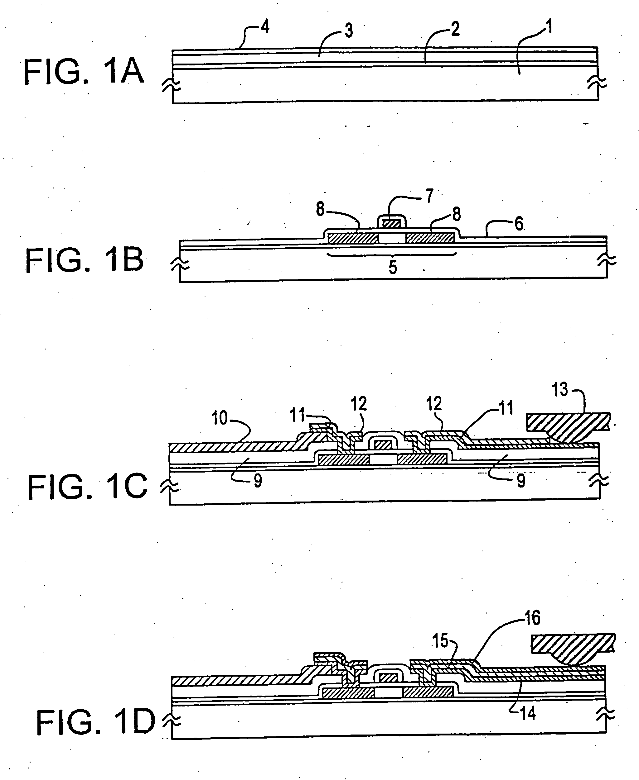
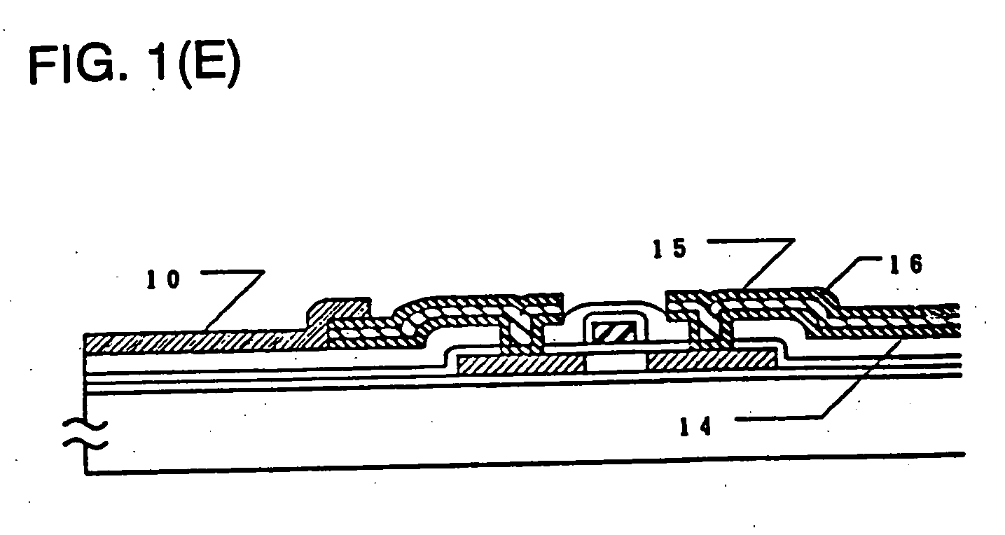
[0029] Example 1 is shown in FIGS. 1, (A)-(D), and 2, (A)-(B). FIGS. 1, (A)-(D), illustrate the sequence in which an electronic circuit having TFTs is fabricated. Description of conventional steps is omitted. First, silicon oxide was deposited as a silicon oxide film 2 forming a base film on a glass substrate 1 made of Corning 7059. An amorphous silicon film 3 having a thickness of 500 to 1500 Å, preferably 500 to 750 Å, was formed on the silicon oxide film 2. A protective layer 4 was formed on the amorphous silicon film 3. The laminate was annealed at 450 to 600° C. for 12 to 48 hours to crystallize the amorphous silicon film. Of course, laser annealing or other similar means can be used for the crystallization (FIG. 1(A)).

[0030] The silicon film was photolithographically patterned into island-shaped semiconductor regions 5. A silicon oxide film 6 having a thickness of 500 to 1500 Å, preferably 800 to 1000 Å, was formed on the semiconductor regions 5 to form a gate oxide film. The...

example 2

[0042] The present example is described by referring to FIG. 1, (A)-(D), which conceptually illustrate the sequence in which an electronic circuit having TFTs is fabricated. Conventional steps are not described herein. First, silicon oxide was deposited as a silicon oxide base film 2 on a glass substrate 1. An amorphous silicon film 3 having a thickness of 100 to 1500 Å, preferably 100 to 750 Å, was formed on the silicon oxide film 2. A protective layer 4 was formed on the amorphous silicon film 3. The laminate was annealed at 450 to 600° C. for 12 to 48 hours to crystallize the amorphous silicon film. Of course, laser annealing or other similar means can also be used for the crystallization (FIG. 1(A)).

[0043] The silicon film was photolithographically patterned into island-shaped semiconductor regions 5. A silicon oxide film 6 having a thickness of 500 to 1500 Å, preferably 800 to 1000 Å, was formed on the semiconductor regions 5 to form a gate oxide film. Then, gate interconnects...

example 3

[0048] The present example is shown in FIGS. 7, (A)-(H). First, silicon oxide was deposited as a silicon oxide film 202 on a glass substrate 201 made of Corning 7059. The silicon oxide film formed a base film and had a thickness of 1000 to 3000 Å. The substrate measured 300 mm×400 mm or 100 mm×100 mm. To form this oxide film, sputtering was effected within oxygen ambient. To make mass production more efficient, TEOS may be decomposed and deposited by plasma CVD.

[0049] Then, amorphous silicon was deposited as a film having a thickness of 300 to 5000 Å, preferably 500 to 1000 Å, by plasma CVD or LPCVD. This film was allowed to stand within an oxidizing ambient at 550 to 600° C. for 24 hours to crystallize the film. This step may also be carried out by laser irradiation. The crystallized silicon film was photolithographically patterned into island-shaped regions 203. A silicon oxide film 104 having a thickness of 700 to 1500 Å was formed by sputtering techniques.

[0050] An aluminum fi...


PUM

PropertyMeasurementUnit
Currentaaaaaaaaaa
Semiconductor propertiesaaaaaaaaaa
Electrical resistivityaaaaaaaaaa

Abstract

An electronic circuit formed on an insulating substrate and having thin-film transistors (TFTs) comprising semiconductor layers. The thickness of the semiconductor layer is less than 1500 Å, e.g., between 100 and 750 Å. A first layer consisting mainly of titanium and nitrogen is formed on the semiconductor layer. A second layer consisting of aluminum is formed on top of the first layer. The first and second layers are patterned into conductive interconnects. The bottom surface of the second layer is substantially totally in intimate contact with the first layer. The interconnects have good contacts with the semiconductor layer.

Description

FIELD OF THE INVENTION [0001] The present invention relates to an electronic circuit which is formed on an insulating substrate and has a thin semiconductor layer of silicon, for example, forming thin-film transistors, the thin semiconductor layer being required to be connected with conductive interconnects. BACKGROUND OF THE INVENTION [0002] Conventional thin-film devices such as insulated-gate FETs use a thin semiconductor film of silicon as an active layer. This layer is about 1500 Å thick. Therefore, where electrodes should be formed on this thin semiconductor film, satisfactory contacts can be made by bringing a metal such as aluminum into direct and intimate contact with the film, in the same way as in the prior art IC fabrication techniques. In these contacts, a silicide such as aluminum silicide is usually formed by a chemical reaction between the aluminum and the semiconductor component such as silicon. Since the semiconductor layer is sufficiently thicker than the silicide...

Claims


Application Information

Patent Timeline
IPC IPC(8): C23C14/34H01L21/28G02F1/133G02F1/136G02F1/1368G09F9/35H01L21/00H01L21/02H01L21/3205H01L21/60H01L21/70H01L21/768H01L21/77H01L21/84H01L23/52H01L23/522H01L23/532H01L27/092H01L27/12H01L29/45H01L29/786H05B33/10H05B33/12H05B33/26H05B44/00
CPCG02F1/1368H01L27/124H01L27/12H01L29/458H01L2924/10253H01L23/53223H01L2924/13091H01L2924/00014H01L2224/45124H01L2924/00H01L2224/48
Inventor MIYAZAKI, MINORUMURAKAMI, AKANECUI, BAOCHUNYAMAMOTO, MUTSUO
Owner SEMICON ENERGY LAB CO LTD
Why Eureka
Try Eureka