Process for production of nitride semiconductor device and nitride semiconductor device

a technology of nitride semiconductor and semiconductor device, which is applied in the direction of crystal growth process, semiconductor laser, polycrystalline material growth, etc., can solve the problems of reducing the light-emitting power of the semiconductor device, the active layer, and the gainn layer at a low temperature of 700° c. to 800° c., so as to facilitate the formation of a smooth surface and low leakage current

Inactive Publication Date: 2005-07-28
BIWA GOSHI +3
View PDF4 Cites 18 Cited by
  • Summary
  • Abstract
  • Description
  • Claims
  • Application Information

AI Technical Summary

Benefits of technology

[0011] The present invention relates to a process for production of a nitride semiconductor device which includes the steps of forming an active layer on a substrate by vapor phase growth at a first growth temperature, and subsequently forming thereon one or more nitride semiconductor layers at a temperature effective to form the additional layer(s) on the active layer without causing, or at least greatly reducing, deterioration of the active layer. In an embodiment, the temperature is maintained at a temperature greater than the first growth temperature by about 250° C. or less, preferably about 150° C. or less. This can prevent breakage of In—N bonds in the active layer which can cause nitrogen voids and the formation of metallic indium. This allows the active layer to retain desirable crystal properties.
[0012] In this regard, the present invention can overcome, for example, the above-mentioned technical problem which arises when an active layer and a nitride semiconductor layer thereon are grown at different temperatures. As a result, the present invention can provide an improved nitride semiconductor device with enhanced characteristics and properties, such as light-emitting characteristics and other suitable properties.
[0013] In an embodiment, the present invention includes a process for production of nitride semiconductor device which includes the steps of forming an active layer on a substrate by vapor phase growth at a first temperature, and subsequently forming thereon one or more nitride semiconductor layers at a second temperature which is greater than the first temperature by about (1350−0.75λ)° C. or less, preferably about (1250−0.75λ)° C. or less, where λ denotes the wavelength (nm) of light emitted by the active layer. Applicants have demonstrated that the process of the present invention conducted at such specific temperatures can effectively protect the active layer from deterioration.
[0015] Applicants have demonstrated that the upper limit of the growth temperature can depend on the wavelength of emitted light as mentioned above and, in addition, the growth temperature of all the nitride semiconductor layers on the active layer can depend on the In content (%) in the compound crystal constituting the active layer. This dependence can be characterized by the linear relationship between temperature and In content, i.e., temperature (1080−4.27X)° C. as previously discussed, which was experimentally found. At such definable temperatures, the active layer can be protected from deterioration.
[0017] In an embodiment, the nitride semiconductor device of the present invention can include the second nitride semiconductor layer formed on the active layer at a temperature no higher than about 900° C. As a result, a smooth surface can be obtained. In an embodiment, the second nitride semiconductor layer can have a thickness larger than about 50 nm, preferably larger than about 100 nm, which can facilitate the formation of a smooth surface.
[0018] In an embodiment, the nitride semiconductor layer is a gallium nitride layer. When grown at about 950° C., a gallium nitride layer is suspect to pitting. Applicants have demonstrated that when grown at a temperature no higher than about 900° C., a gallium nitride layer has a smooth surface substantially free of pitting. It is believed this is because the surface diffusion length of Group III atoms is short at such a low temperature. As a result, a semiconductor device fabricated according to an embodiment of the present invention has a low leakage current.

Problems solved by technology

However, growing the GaInN layer (as the well layer) at a low temperature of 700° C. to 800° C. and then growing the GaN layer or AlGaN layer (as the barrier layer) at a high temperature of about 1000° C. can be problematic.
In this regard, the underlying GaInN layer can deteriorate, and thus decrease the light-emitting power of the semiconductor device.
This results in an active layer with poor crystal properties due to breakage of In—N bonds in the InGaN layer which gives rise to nitrogen voids and the formation of metallic indium.
Marked deterioration in performance occurs particularly in those devices emitting visible light whose active layer and p-type GaN layer are grown at greatly different temperatures.
However, this is not a complete solution because the InGaN active layer is still subject to deterioration so long as another layer is formed at a high temperature on the GaN cap layer which has been formed at a low temperature.
Moreover, there is another disadvantage in growing a layer on the active layer at a low temperature for its protection.
That is, gallium nitride compound semiconductors are liable to pitting when grown at a temperature lower than an optimal growth temperature.

Method used


Image

  • Process for production of nitride semiconductor device and nitride semiconductor device
  • Process for production of nitride semiconductor device and nitride semiconductor device
  • Process for production of nitride semiconductor device and nitride semiconductor device

Examples


example 1

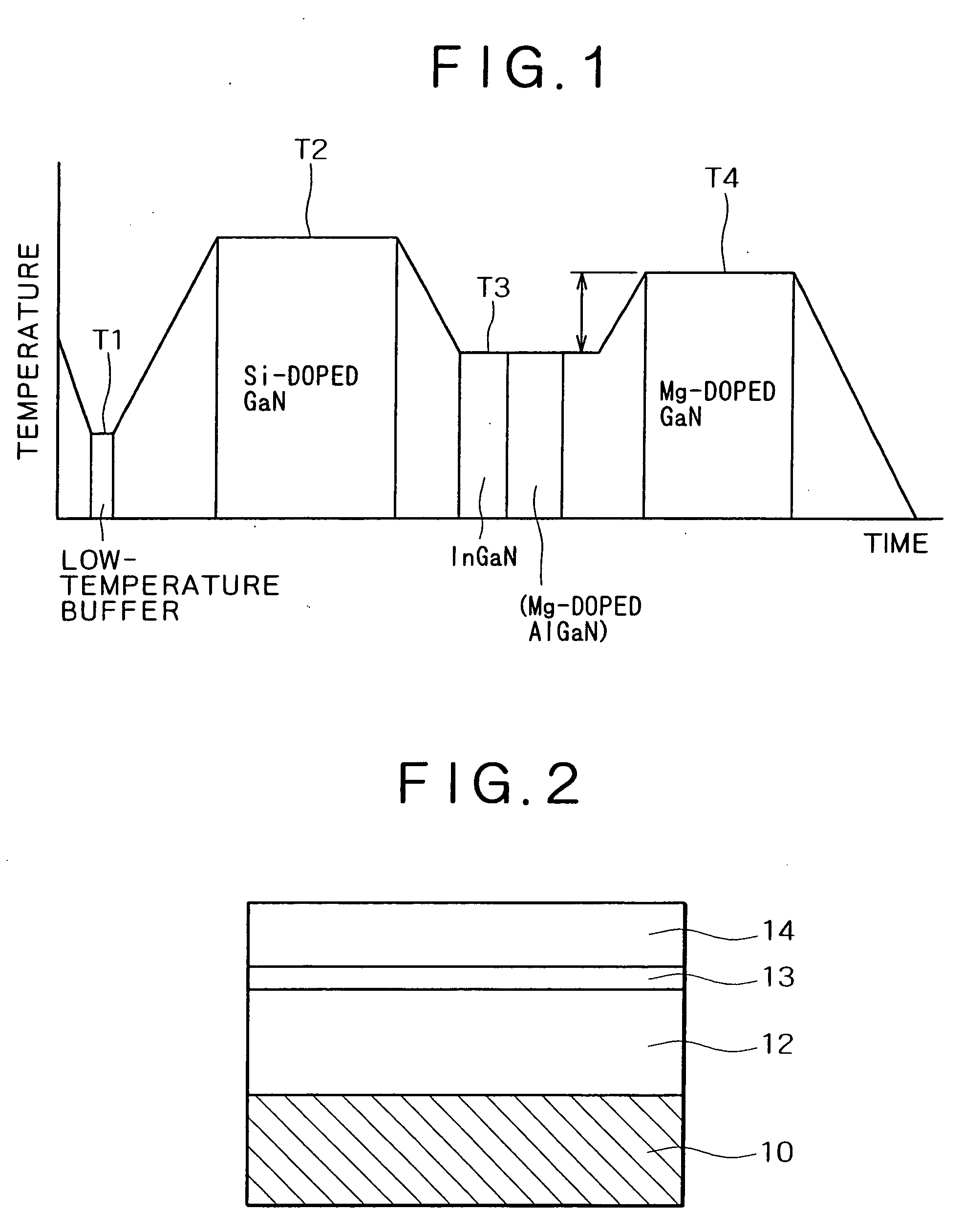
[0034] This example demonstrates the process for production of a nitride semiconductor device according to an embodiment of the present invention as shown in FIGS. 1 to 3.

[0035]FIG. 1 is a diagram showing the growth temperature which varies with time for different layers. It is noted that the initial growth temperature (T1) for the buffer layer is about 500° C. as shown in FIG. 1. The growth temperature is raised to T2 (about 1020° C.) for the silicon-doped n-type GaN layer. With the supply of trimethylgallium suspended temporarily, the growth temperature is lowered to T3 (about 730° C.). With the growth temperature kept at 730° C., an active layer of InGaN (30 angstroms (Å) thick) is grown from trimethylgallium (as a gallium source) and trimethylindium (as an indium source) after the carrier gas has been switched from a mixture to nitrogen.

[0036] After the active layer of InGaN has been formed, the magnesium-doped AlGaN layer is grown thereon at the growth temperature of T3. Subs...

example 2

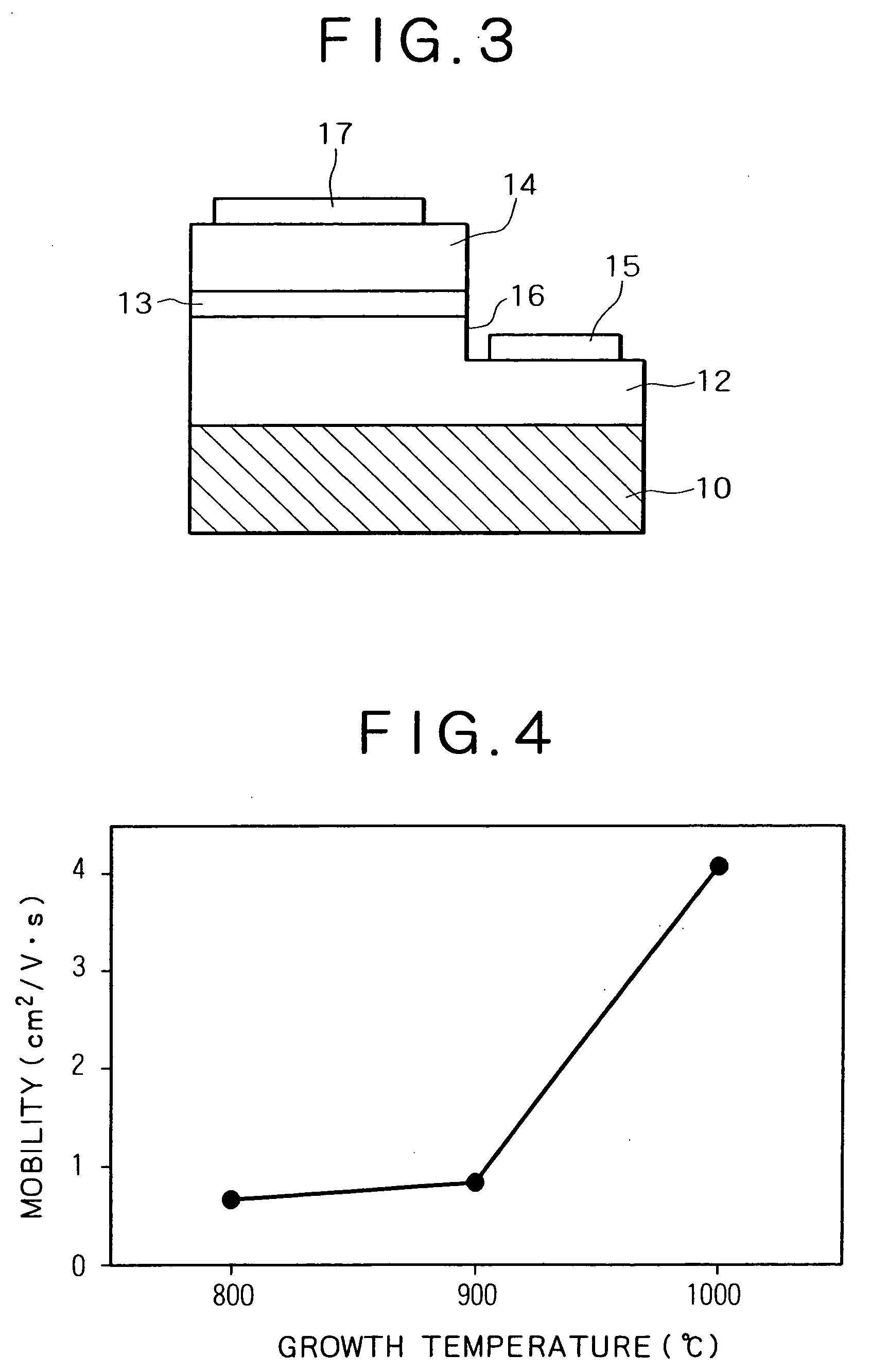
[0044] This example demonstrates the process for production of a GaN-based semiconductor light-emitting device according to an embodiment of the present invention that has a similar structure as that in Example 1. This example is based on the fact that the wavelength of the light emitted from the GaN semiconductor light-emitting device varies depending on the growth temperature of the nitride semiconductor layer formed on the active layer.

[0045] Applicants have discovered through experimentation that the wavelength of the light emitted from the GaN semiconductor light-emitting device varies depending on the growth temperature of the nitride semiconductor layer formed on the active layer. Applicants conducted experiments on several kinds of GaN-based light-emitting diodes, each having the same structure as in Example 1 (or including an n-type GaN layer, an InGaN layer, and a p-type GaN layer) but differing in the growth condition for the active layer. The resulting samples were test...

example 3

[0048] This example demonstrates a GaN-based semiconductor laser in which the active layer is a compound crystal of indium. The process for its production will be explained with reference to FIGS. 6 and 7.

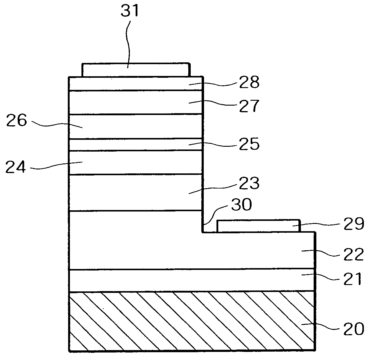
[0049] First, a sapphire substrate 20 (whose principal plane is c-plane) undergoes thermal cleaning at about 1050° C. in the same way as in Example 1. On the substrate is grown a GaN or AlN buffer layer at about 510° C. With the reaction temperature raised to about 1020° C., an undoped GaN layer 21 (1 micron thick) and a silicon-doped n-type GaN layer 22 (3 microns thick) are grown sequentially. Silicon is introduced in the form of silane gas.

[0050] With the Si-doped n-type GaN layer 22 formed, the reaction chamber is supplied with NH3 (as a nitrogen source), trimethylgallium (Ga(CH3)3 as a gallium source), and trimethylaluminum (Al(CH3)3 as an aluminum source), so that an n-type AlGaN cladding layer 23 is grown.

[0051] With the supply of NH3 continued but the supply of trimethyl...


PUM


Abstract

Disclosed herein is a process for production of a nitride semiconductor device having good characteristic properties (such as light-emitting performance). The process does not thermally deteriorate the active layer while nitride semiconductor layers are being grown on the active layer. The process consists of forming an active layer on a substrate by vapor phase growth at a first growth temperature, and subsequently forming thereon one or more nitride semiconductor layers at a temperature which is lower than said first growth temperature plus 250° C. The process yields a nitride semiconductor device in which the active layer retains its good crystal properties, without nitrogen voids and metallic indium occurring therein due to breakage of In—N bonds.

Description

CROSS REFERENCE TO RELATED APPLICATIONS [0001] The present invention is a continuation of U.S. patent application Ser. No. 10 / 127,153 filed Nov. 28, 2002, which claims priority to Japanese Patent Document No. P2001-121689 filed on Apr. 19, 2001, the disclosures of which are herein incorporated by reference.BACKGROUND OF THE INVENTION [0002] The present invention generally relates to a process for production of a nitride semiconductor device. More specifically, the present invention relates to growing on a substrate a nitride semiconductor, such as gallium nitride compound semiconductor that can be used in a variety of suitable applications, such as a light-emitting device including, for example, a semiconductor diode, a semiconductor laser or the like. [0003] Known semiconductors include nitride compound semiconductors (such as GaN, AlGaN, and GaInN) composed of elements belonging to Groups III and V and have a broad bandgap width ranging from 1.8 eV to 6.2 eV. In theory, this makes...

Claims


Application Information

Patent Timeline
IPC IPC(8): C30B25/02H01L21/205H01L21/338H01L29/778H01L29/812H01L33/00H01L33/06H01L33/32H01S5/323H01S5/343
CPCC30B25/02C30B29/403C30B29/406H01L33/007H01L21/0242H01L21/0262H01L21/02505H01L21/0254H01L21/02576H01L21/02579H01L21/02458
Inventor BIWA, GOSHIOKUYAMA, HIROYUKIDOI, MASATOOOHATA, TOYOHARU
Owner BIWA GOSHI
Why Eureka
Try Eureka