Semiconductor structures using a group III-nitride material system with reduced phase separation and method of fabrication

a technology of nitride and material, applied in the field of semiconductor structure and process, can solve the problems of increased threshold current, reduced light emission efficiency, large operating current, etc., and achieve the effects of reducing phase separation, reducing defect densities, and improving emission efficiency

Inactive Publication Date: 2005-07-28
PANASONIC CORP
View PDF5 Cites 8 Cited by
  • Summary
  • Abstract
  • Description
  • Claims
  • Application Information

AI Technical Summary

Benefits of technology

[0010] The present invention substantially overcomes the limitations of the prior art by providing a semiconductor structure which substantially reduces defect densities by materially reducing phase separation between the layers of the structure. This in turn permits substantially improved emission efficiency. In general, the present invention utilizes group III-nitride quaternary and pentenary material systems and methods.
[0011] To reduce phase separation, it has been found possible to provide a semiconductor device with InGaAlN layers having homogeneous In content, Al content, Ga content distribution in each layer. In a light emitting device, this permits optical absorption loss and waveguide scattering loss to be reduced, resulting in a high efficiency light emitting device.
[0012] A quaternary material system such as InGaAlN has been found to provide, reproducibly, sufficient homogeneity to substantially reduce phase separation where the GaN mole fraction, x, and the AlN mole fraction, y, of all the constituent layers in the semiconductor structure satisfy the condition that x+1.2y nearly equals a constant value.

Problems solved by technology

The defects result from phase separation and act as absorption centers for the lasing light, causing decreased light emission efficiency and increased threshold current.
The result is that the operating current becomes large, which in turn causes reliability to suffer.
Therefore, ultraviolet light which has an energy level higher than 3.5 eV cannot be obtained by using an InGaN active layer.
This presents difficulties, since ultraviolet light is attractive as a light source for the optical pick up device in, for example, higher density optical disc memory systems and other devices.
As noted above, a typical prior art solution to these problems has been to increase drive current, thus reducing the life of the semiconductor device.

Method used


Image

  • Semiconductor structures using a group III-nitride material system with reduced phase separation and method of fabrication
  • Semiconductor structures using a group III-nitride material system with reduced phase separation and method of fabrication
  • Semiconductor structures using a group III-nitride material system with reduced phase separation and method of fabrication

Examples


first embodiment

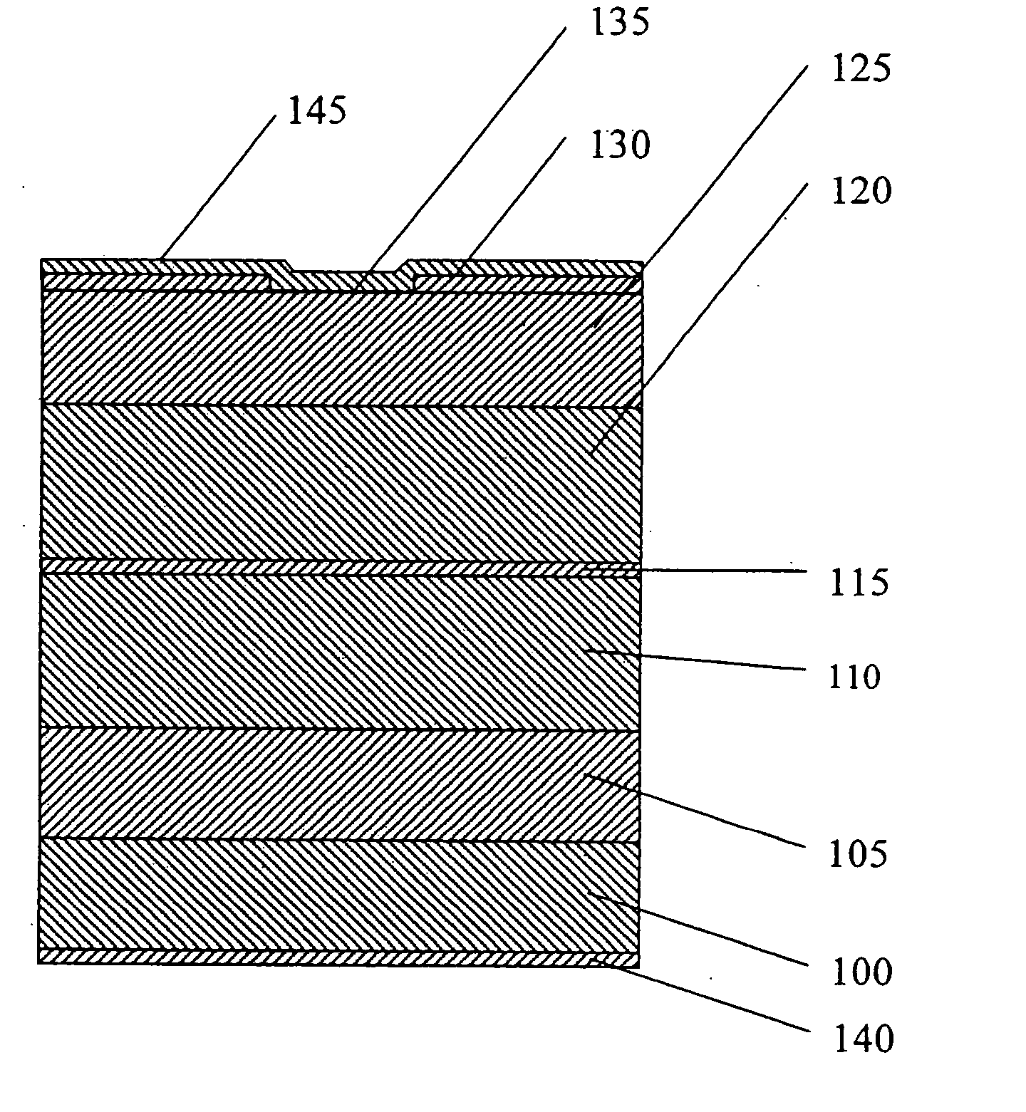
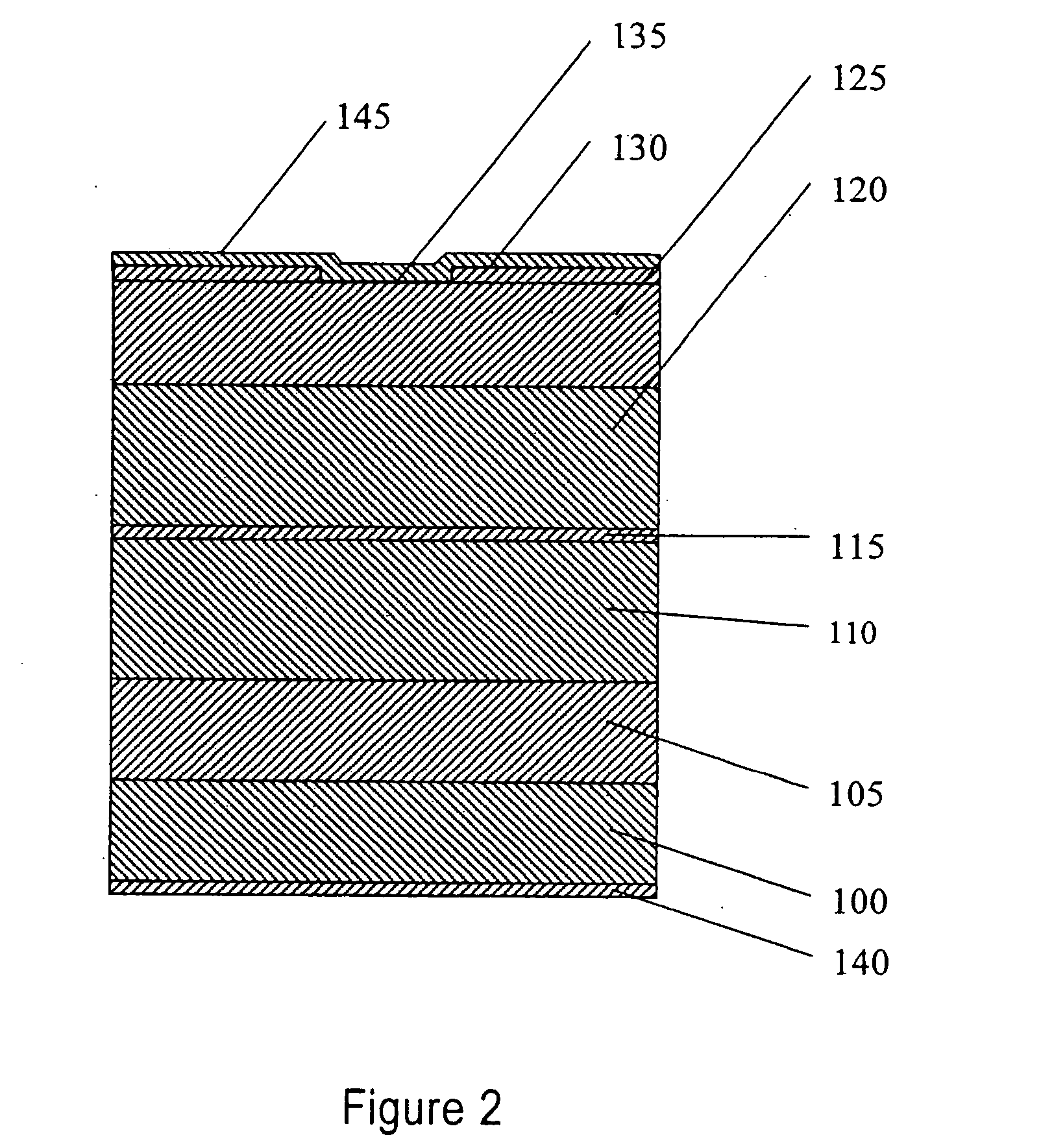
[0081] Referring first to FIG. 2, shown therein, in cross-sectional view is a semiconductor structure according to the invention. For purposes of illustration, the semiconductor structure shown in many of the Figures will be a laser diode, although the present invention has application to a number of device types. With particular reference to FIG. 1, an n-type GaN substrate 100 is provided and an n-type GaN first cladding layer 105 (typically 0.5 μm thick) is formed thereon. Thereafter, a second cladding layer 110, typically of an n-type In0.05Ga0.75Al0.2N material which may be on the order of 1.5 μm thick, is formed thereon, followed by a multiple quantum well active layer 115 which in an exemplary arrangement may comprise three quantum well layers of In0.01Ga0.96Al0.03N material on the order of 35A thick together with four barrier layers of In0.02Ga0.85Al0.13N material on the order of 35A thick, arranged as three pairs. Next, a third cladding layer 120 of a p-type In0.05Ga0.75Al0....

second embodiment

[0093]FIG. 6 shows in graph form the emitted light versus drive current characteristics of a laser diode in accordance with the The laser diode is driven with a cw current. The threshold current is found to be 32.5 mA.

[0094] Referring next to FIGS. 7A-7E, a summary of the key fabrication steps is shown for an exemplary device of a semiconductor laser diode in accordance with the second embodiment.

[0095] Referring first to FIGS. 7A and 7B, the formation of the first and second cladding layers 105 and 110 on an n-type GaN substrate 100, together with the three-pair multiple quantum well active layer 115 are the same as for the first embodiment. Thereafter, the third and fourth cladding layers 120 and 125 are formed and then partially removed—typically by etching—to create a ridge structure 500. As before, in an exemplary embodiment the various layers are formed successively by either the MOCVD or the MBE method.

[0096] Then, as shown in FIG. 7C-7E, a silicon dioxide layer 130 is for...

third embodiment

[0100]FIG. 9 shows a plot of the emitted light versus drive current characteristics of the laser diode in accordance with the The laser diode is driven with a pulsed current with a duty cycle of 1%. The threshold current density is found to be 5.0 kA / cm2.

[0101]FIGS. 10A-10D show a series of the fabrication steps of a semiconductor laser diode in one example of the third embodiment. It will be appreciated that the fabrication steps are the same as those described in connection with FIGS. 4A-4D, and therefore are not further described.

[0102] Referring next to FIG. 11, a fourth embodiment of the present invention may be better appreciated. The fourth embodiment, like the third embodiment, is designed to emit blue light and therefore has the same mole fractions as the third embodiment. However, like the second embodiment, the fourth embodiment is configured to provide a ridge structure to serve as a waveguide. Because the mole fractions are similar to those of FIG. 8, similar elements...


PUM


Abstract

Group III-nitride quaternary and pentenary material systems and methods are disclosed for use in semiconductor structures, including laser diodes, transistors, and photodetectors, which reduce or eliminate phase separation and provide increased emission efficiency. In an exemplary embodiment the semiconductor structure includes a first ternary, quaternary or pentenary material layer using BInGaAlN material system of a first conduction type formed substantially without phase separation, and a quaternary or pentenary material active layer using BInGaAlN material system substantially without phase separation, and a third ternary, quaternary or pentenary material layer using BInGaAlN material system of an opposite conduction type formed substantially without phase separation.

Description

RELATED CASES [0001] This application is a continuation in part of U.S. patent application Ser. No. 09 / 276,886 filed Mar. 26, 1999, entitled “SemiConductor Structures Using A Group III-Nitride Quaternary Material System with Reduced Phase Separation and Method of Fabrication” and Ser. No. 09 / 365,105 filed Jul. 30, 1999, entitled “SemiConductor Structures Using A Group III-Nitride Quaternary Material System with Reduced Phase Separation and Method of Fabrication”.FIELD OF THE INVENTION [0002] This application relates to semiconductor structures and processes, and particularly relates to group III-nitride materials systems and methods such as might be used in laser diodes. BACKGROUND OF THE INVENTION [0003] The development of the blue laser light source has heralded the next generation of high density optical devices, including disc memories, DVDs, and so on. FIG. 1 shows a cross sectional illustration of a prior art semiconductor laser device. (S. Nakamura, MRS BULLETIN, Vol. 23, No....

Claims


Application Information

Patent Timeline
Patent Type & Authority Applications(United States)
IPC IPC(8): H01L29/201H01L31/103H01L33/32H01S5/323H01S5/343
CPCB82Y20/00H01L29/201H01L31/1035H01L33/32H01S2304/00H01S5/32H01S5/32341H01S5/34333H01S5/22
Inventor TAKAYAMA, TORUBABA, TAKAAKIHARRIS, JAMES S. JR.
Owner PANASONIC CORP
Why Eureka
Try Eureka