Coating forming agent for reducing pattern dimension and method of forming fine pattern therewith

Inactive Publication Date: 2005-08-11
TOKYO OHKA KOGYO CO LTD
View PDF4 Cites 22 Cited by
  • Summary
  • Abstract
  • Description
  • Claims
  • Application Information

AI Technical Summary

Benefits of technology

[0011] An object of the present invention is to provide an over-coating agent for forming fine patterns. It can remarkably increase the thermal shrinkage of the over-coating agent in the heat treatment, thereby to form finer patterns effectively, and has high ability to c

Problems solved by technology

However, in these methods, it is difficult to control the thickness of layers to be formed on the sidewalls of resist patterns.
In addition, the in-plane heat dependency of wafers is as great as ten-odd nanometers per degree Celsius, so it is extremely difficult to keep the in-plane uniformity of wafers by means of the heater employed in current fabrication of semiconductor devices and this leads to the problem of occurrence of significant variations in pattern dimensions.
On the other hand, it is difficult to control the resist deformation and flui

Method used


Image

  • Coating forming agent for reducing pattern dimension and method of forming fine pattern therewith
  • Coating forming agent for reducing pattern dimension and method of forming fine pattern therewith
  • Coating forming agent for reducing pattern dimension and method of forming fine pattern therewith

Examples


Example

Example 1

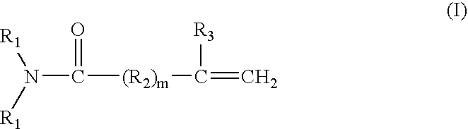
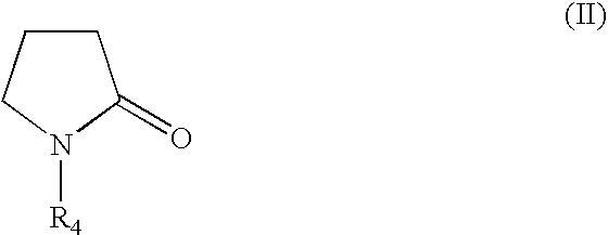
[0080] A copolymer of acrylic acid and vinylpyrrolidone [5.83 g; acrylic acid / vinylpyrrolidone=2:1 (polymerization ratio)], triethanolamine (0.53 g), acrylamide (0.58 g) and “PLY-SURF A210G”, product of Dai-ichi Kogyo Seiyaku Co., as phosphate esters of polyoxyethylene surfactant (0.06 g) were dissolved in water (93 g) to prepare an over-coating agent.

[0081] A substrate was whirl coated with a positive-acting photoresist TArF-7a-52 EM (product of Tokyo Ohka Kogyo Co., Ltd.), and baked at 115° C. for 90 seconds to form a photoresist layer in a thickness of 0.40 μm.

[0082] The photoresist layer was exposed with a laser exposure unit (Nikon S-302 of Nikon Corp.), subjected to heat treatment at 100° C. for 90 seconds and developed with an aqueous solution of 2.38 mass % TMAH (tetramethylammonium hydroxide) to form photoresist patterns which defined hole patterns with an each diameter of 161.0 nm.

[0083] Then above-described over-coating agent was applied onto the substrate in...

Example

Example 2

[0084] A copolymer of acrylic acid and vinylpyrrolidone [6.14 g; acrylic acid / vinylpyrrolidone=2:1 (polymerization ratio)], glycerol (0.18 g), acrylamide (0.62 g) and “PLYSURF A210G”, product of Dai-ichi Kogyo Seiyaku Co., as phosphate esters of polyoxyethylene surfactant (0.06 g) were dissolved in water (93 g) to prepare an over-coating agent.

[0085] Then above-described over-coating agent was applied onto the substrate including the hole patterns (each diameter of patterns: 161.0 nm) which was prepared in the same manner as described in EXAMPLE 1, and subjected to heat treatment at 150° C. for 60 seconds. Subsequently, the over-coating agent was removed using pure water at 23° C. The each diameter of the hole patterns was reduced to 121.7 nm.

Example

Example 3

[0086] A copolymer of acrylic acid and vinylpyrrolidone [6.14 g; acrylic acid / vinylpyrrolidone=2:1 (polymerization ratio)], glycerol (0.18 g), methacrylamide (0.62 g) and “PLYSURF A210G”, product of Dai-ichi Kogyo Seiyaku Co., as phosphate esters of polyoxyethylene surfactant (0.06 g) were dissolved in water (93 g) to prepare an over-coating agent.

[0087] Then above-described over-coating agent was applied onto the substrate including the hole patterns (each diameter of patterns: 161.0 nm) which was prepared in the same manner as described in EXAMPLE 1, and subjected to heat treatment at 150° C. for 60 seconds. Subsequently, the over-coating agent was removed using pure water at 23° C. The each diameter of the hole patterns was reduced to 122.6 nm.

[Second Type of the Over-Coating Agent for Forming Fine Patterns]


PUM


Abstract

It is disclosed an over-coating agent for forming fine patterns which is applied to cover a substrate having thereon photoresist patterns and allowed to shrink under heat so that the spacing between adjacent photoresist patterns is lessened, with the applied film of the over-coating agent being removed substantially completely to form or define fine trace patterns, further characterized by containing either a water-soluble polymer and an amide group-containing monomer or a water-soluble polymer which contains at least (meth)acrylamide as a monomeric component. Also disclosed is a method of forming fine-line patterns using any one of said over-coating agents. According to the invention, the thermal shrinkage of the over-coating agent for forming fine patterns in the heat treatment can be extensively increased, and one can obtain fine-line patterns which exhibit good profiles while satisfying the characteristics required of semiconductor devices.

Description

TECHNICAL FIELD [0001] This invention relates to an over-coating agent for forming fine patterns in the field of photolithographic technology and a method of forming fine-line patterns using such agent. More particularly, the invention relates to an over-coating agent for forming or defining fine-line patterns, such as hole patterns and trench patterns, that can meet today's requirements for higher packing densities and smaller sizes of semiconductor devices. BACKGROUND ART [0002] In the manufacture of electronic components such as semiconductor devices and liquid-crystal devices, there is employed the photolithographic technology which, in order to perform a treatment such as etching on the substrate, first forms a film (photoresist layer) over the substrate using a so-called radiation-sensitive photoresist which is sensitive to activating radiations, then performs exposure of the film by selective illumination with an activating radiation, performs development to dissolve away the...

Claims


Application Information

Patent Timeline
IPC IPC(8): H01L21/027G03F7/40
CPCH01L2051/0063G03F7/40H10K85/6565
Inventor SUGETA, YOSHIKIKANEKO, FUMITAKETACHIKAWA, TOSHIKAZU
Owner TOKYO OHKA KOGYO CO LTD
Why Eureka
Try Eureka