Semiconductor device and manufacturing method therefor

a technology of semiconductors and semiconductors, applied in the direction of semiconductor devices, electrical appliances, transistors, etc., can solve the problems of increasing leakage current, reducing film thickness, and unable to ensure the desired drain current level

Inactive Publication Date: 2005-09-15
KK TOSHIBA
View PDF3 Cites 69 Cited by
  • Summary
  • Abstract
  • Description
  • Claims
  • Application Information

AI Technical Summary

Benefits of technology

[0042] According to another aspect of the present invention, a semiconductor device comprises a silicon substrate, and a CMOSFET formed on the silicon substrate and made up of an NMOSFET and a PMOSFET. A gate dielectric film of the NMOSFET and a gate dielectric film of the PMOSFET each have a laminated structure including a first insulating film and a second insulating film. The first insulating film is formed on the silicon substrate, and the second insulating film is formed on the first insulating film. A gate electrode of the NMOSFET includes an n-type silicon film and a first metal silicide film. The n-type silicon film is formed on the gate dielectric film of the NMOSFET, and the first metal silicide film is formed on the n-type silicon film. A gate electrode of the PMOSFET has a laminated structure including a metal film and a second metal silicide film. The metal film is formed on the gate dielectric film of the PMOSFET, and the second metal silicide film is formed on the metal film. The second insulating film is a high dielectric constant insulating film, and is not formed on sidewalls of the gate electrodes of the NMOSFET and the PMOSFET.
[0043] According to other aspect of the present invention, in a method for manufacturing a semiconductor device including a CMOSFET made up of an NMOSFET and a PMOSFET, a gate dielectric film is formed on a silicon substrate in which are provided a element isolation insulating film, an n-type diffusion layer region, and a p-type diffusion layer region. The gate dielectric film includes a high dielectric constant insulating film. A silicon film is formed on the gate dielectric film. N-type impurities is implanted in the portion of the silicon film in an NMOSFET region for the NMOSFET, The silicon film is processed to form an n-type silicon film pattern and an undoped silicon film pattern each having a gate electrode shape. Portions of the gate dielectric film other than those under the n-type silicon film pattern and the undoped silicon film pattern are removed. After the step of removing the portions of the gate dielectric film, a first sidewall insulating film is formed on the entire surface of the silicon substrate. Impurities are implanted in the silicon substrate using the n-type silicon film pattern and the undoped silicon film pattern as masks to form an n-type extension region and a p-type extension region. A second sidewall insulating film is formed on the first sidewall insulating film. Portions of the first and second sidewall insulating films other than those on sidewalls of the n-type silicon film pattern and the undoped silicon film pattern are removed. Impurities are implanted in the silicon substrate using the n-type silicon film pattern and the undoped silicon film pattern as masks to form an n-type source and an n-type drain regions (an n-type source/drain region) and a p-type source and a p-type drain regions (a p-type source/drain region). The n-type silicon film pattern and the undoped silicon film pattern have the first and second sidewall insulating films on the sidewalls. A first metal silicide film is formed on the n-type source/drain region and the p-type source/drain region. After the step of forming the first metal silicide film, an interlayer insulating film is formed on the silicon substrate such that the n-type silicon film pattern and the undoped silicon film pattern are buried under the interlayer insulating film. The interlayer insulating film is processed so as to expose surfaces of the n-type silicon film pattern and the undoped silicon film pattern. The undoped silicon film pattern is etched to a predetermined film thickness. A metal film is formed on the entire surface of the silicon substrate. A heat treatment is performed so as to transform an upper portion of the n-type silicon film pattern and all portions of the undoped silicon film pattern into second metal silicide films formed of a silicide of the metal film.
[0044] According to other aspect of the present invention, in a method for manufacturing a semiconductor device includes a CMOSFET made up of an NMOSFET and a PMOSFET, a gate dielectric film is formed on a silicon substrate in which are provided a element isolation insulating film, an n-type diffusion layer region, and a p-type diffusion layer region. The gate dielectric film includes a high dielectric constant insulating film. A silicon film is formed on the gate dielectric film. N-type impurities are implanted in the portion of the silicon film in an NMOSFET region for the NMOSFET. The silicon film is processed to form an n-type silicon film pattern and an undoped silicon film pattern each having a gate electrode shape. Portions of the gate dielectric film other than those under the n-type silicon film pattern and the undoped silicon film pattern are removed. After the step of removing the portions of the gate dielectric film, a first sidewall insulating film is formed on the entire surface of the silicon substrate. Impurities are implanted in the silicon substrate using the n-type silicon film pattern and the undoped silicon film pattern as masks to form an n-type extension region and a p-type extension region. a second sidewall insulating film is formed on the first sidewall insulating film. Portions of the first and second sidewall insulating films other than those on sidewalls of the n-type silicon film pattern and the undoped silicon film pattern are removed. Impurities are implanted in the silicon substrate using the n-type silicon film pattern and the undoped silicon film pattern as masks to form an n-type source/drain region and a p-type source/drain region. The n-type silicon film pattern and the undoped silicon film pattern have the first and second sidewall insulating films on the sidewalls. A first metal silicide film is formed on the n-type source/drain region and the p-type source/drain region. After the step of forming the first metal silicide film, an interlayer insulating film is formed on the silicon substrate such that the n-type silicon film pattern and the undoped silicon film pattern are buried under the interlayer insulating film. The interlayer insulating film is processed so as to expose surfaces of the n-type silicon film pattern and the undoped silicon film pattern. A first metal film is formed on the entire surface of the silicon substrate. A heat treatment is performed so as to transform an upper portion of the n-type silicon film pattern and an upper portion of the undoped silicon film pattern into second metal silicide films formed of a silicide of the first metal film. The second metal silicide film on the undoped silicon film pattern is removed. A second metal film and a third metal film are sequentially formed on the undoped silicon film pattern. A heat treatment is performed so as to cause the undoped silicon film pattern, and the second and third metal films to react with one another, and thereby form a laminated structure on the gate dielectric film. The laminated structure is made up of the second metal film and a third metal silicide film laminated onto the second metal film. The third metal silicide film is formed of a silicide of the third metal film.
[0045] According to other aspect of the present invention, in a method for manufacturing a semiconductor device includes a CMOSFET made up of an NMOSFET and a PMOSFET, a gate dielectric film is formed on a silicon substrate in which are provided a element isolation insulating film, an n-type diffusion layer region, and a p-type diffusion layer region. The gate dielectric film includes a high dielectric constant insulating film. A silicon film is formed on the gate dielectric film. N-type impurities are implanted in the portion of the silicon film in an NMOSFET region for the NMOSFET. The silicon film is processed to form an n-type silicon film pattern and an undoped silicon film pattern each having a gate electrode shape. Portions of the gate dielectric film other than those under the n-type silicon film pattern and the undoped silicon film pattern are removed. After the step of removing the portions of the gate dielectric film, a first sidewall insulating film is formed on the entire surface of the silicon substrate. Impurities are implanted in the silicon substrate using the n-type silicon f

Problems solved by technology

However, reducing the film thickness of a gate dielectric film formed of such a material increases the leakage current.
Furthermore, the PMOSFET has a smaller inversion capacitance than the NMOSFET, making it impossible to ensure a desired drain current level (see, e.g., T. Aoyama et al., International Workshop on Gate Insulator, 2003, p.
However, since metal electrodes have poor heat resistance as compared to silicon electrodes, it is not possible to form a transistor with metal electrodes using the above conventional process.
However, if the gate electrodes of the NMOSFET and the PMOSFET are formed of the same type of metal film, the threshold voltage of one of the FETs cannot be set to an appropriate value.
This problem arises not only with NMOS gate electrodes formed of a titanium nitride film but also with NMOS gate electrodes of other materials whose Fermi level lies close to the middle of the bandgap of silicon, such as nickel silicide and cobalt silicide, when these electrodes are used with a high dielectric constant insulating film.
This means that this problem is considered to occur only when a high dielectric constant insulating film is used as a g

Method used


Image

  • Semiconductor device and manufacturing method therefor
  • Semiconductor device and manufacturing method therefor
  • Semiconductor device and manufacturing method therefor

Examples


first embodiment

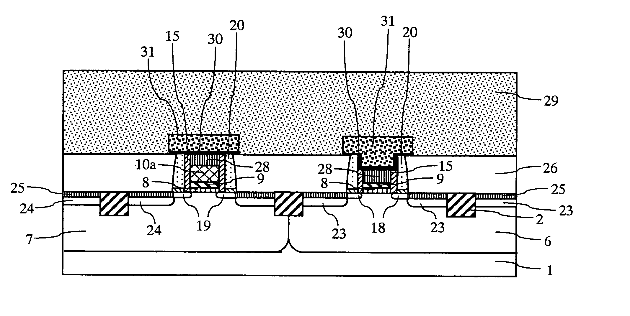
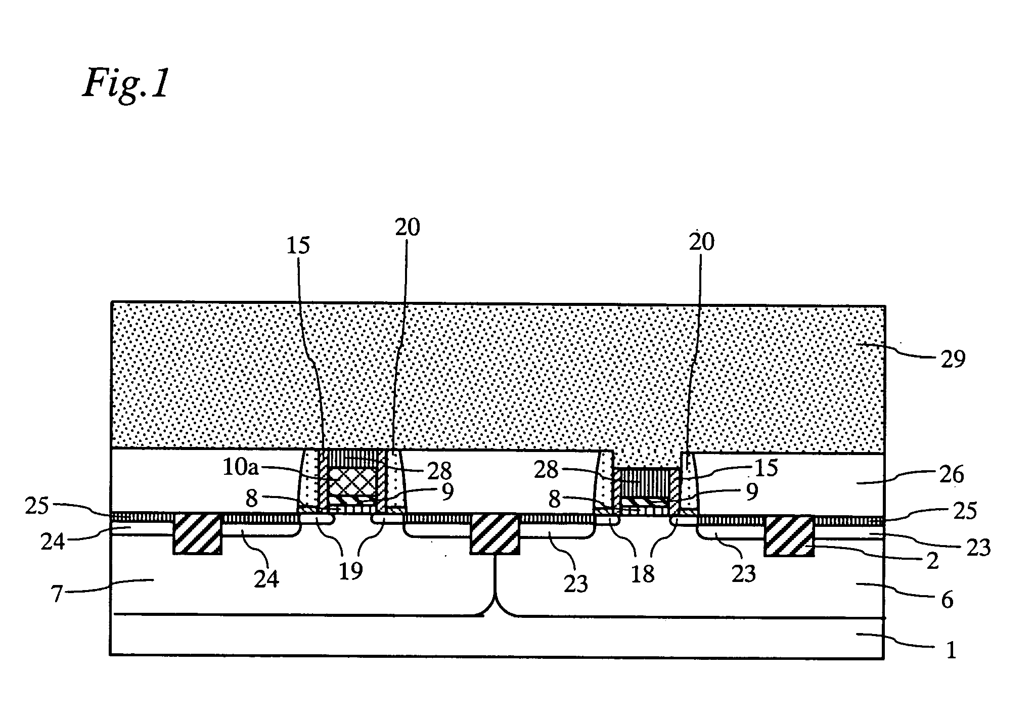
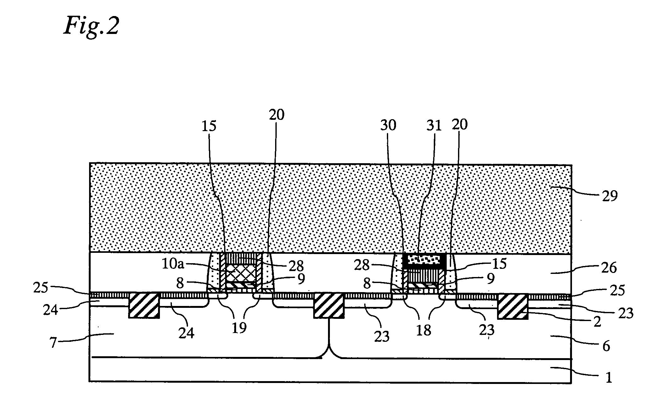
[0094]FIG. 1 is a cross-sectional view of a semiconductor device according to a first embodiment of the present invention.

[0095] Referring to the figure, a element isolation insulating film 2 is formed around the device regions in a silicon substrate 1. Within the device regions are formed an n-type diffusion layer region 6, a p-type diffusion layer region 7, a p-type extension region 18, an n-type extension region 19, a p-type source / drain region 23, an n-type source / drain region 24, and a nickel silicide film 25.

[0096] The gate dielectric film formed on each channel is made up of a first insulating film and a second insulating film formed on the first insulating film. The first insulating film is a silicon oxide film 8 acting as an underlying interface layer, while the second insulating film is a hafnium silicon oxynitride film 9, which is a high dielectric constant insulating film.

[0097] The n-type gate electrode is made up of an n-type silicon film 10a and a nickel silicide f...

second embodiment

[0135]FIG. 13 is a cross-sectional view of a semiconductor device according to a second embodiment of the present invention.

[0136] Referring to the figure, a element isolation insulating film 102 is formed around the device regions in a silicon substrate 101. Within the device regions are formed an n-type diffusion layer region 106, a p-type diffusion layer region 107, a p-type extension region 1018, an n-type extension region 1019, a p-type source / drain region 1023, an n-type source / drain region 1024, and a nickel silicide film 1025.

[0137] The gate dielectric film formed on each channel is made up of a first insulating film and a second insulating film formed on the first insulating film. The first insulating film is a silicon oxynitride film 108a acting as an underlying interface layer, while the second insulating film is a hafnium silicate film 109a, which is a high dielectric constant insulating film.

[0138] The n-type gate electrode is made up of an n-type silicon film 1010a ...

third embodiment

[0160] FIGS. 18 to 24 are cross-sectional views of semiconductor devices according to a third embodiment of the present invention.

[0161] Referring to FIG. 18, a element isolation insulating film 202 is formed around the device regions in a silicon substrate 201. Within the device regions are formed an n-type diffusion layer region 206, a p-type diffusion layer region 207, a p-type extension region 2018, an n-type extension region 2019, a p-type source / drain region 2023, an n-type source / drain region 2024, and a nickel silicide film 2025.

[0162] The gate dielectric film formed on each channel is made up of a first insulating film and a second insulating film formed on the first insulating film. The first insulating film is a silicon oxide film 208 acting as an underlying interface layer, while the second insulating film is a high dielectric constant insulating film made up of a hafnium oxide film 209b and a silicon nitride film 209c formed on the hafnium oxide film 209b.

[0163] The ...


PUM


Abstract

An element isolation dielectric film is formed around device regions in a silicon substrate. The device regions are an n-type diffusion region, a p-type diffusion region, a p-type extension region, an n-type extension region, a p-type source/drain region, an n-type source/drain region, and a nickel silicide film. Each gate dielectric film includes a silicon oxide film and a hafnium silicate nitride film. The n-type gate electrode includes an n-type silicon film and a nickel silicide film, and the p-type gate electrode includes a nickel silicide film. The hafnium silicate nitride films are not on the sidewalls of the gate electrodes.

Description

BACKGROUND OF THE INVENTION [0001] 1. Field of the Invention [0002] The present invention relates to a semiconductor device and a manufacturing method therefor, and more particularly to a semiconductor device including a CMOSFET made up of an NMOSFET and a PMOSFET formed on a silicon substrate, and a manufacturing method therefor. [0003] 2. Background Art [0004] In recent years, the integration density of semiconductor integrated circuit devices has considerably increased. As such, devices such as transistors in MOS (Metal Oxide Semiconductor) devices have been miniaturized and enhanced in performance. Especially, gate dielectric films, which are a component of the MOS structure, have become thinner and thinner to accommodate the miniaturization, high-speed operation, and lower-voltage operation of the transistors. [0005] Conventionally, a silicon oxide (SiO2) film or a silicon oxynitride (SiON) film is used as a gate dielectric film. However, reducing the film thickness of a gate d...

Claims


Application Information

Patent Timeline
IPC IPC(8): H01L21/8238H01L29/76
CPCH01L21/28052H01L21/28097H01L21/28114H01L21/28247H01L29/42376H01L21/823835H01L29/518H01L29/66545H01L29/6659H01L29/7833H01L29/513
Inventor AOYAMA, TOMONORI
Owner KK TOSHIBA
Why Eureka
Try Eureka