Electron beam apparatus, a device manufacturing method using the same apparatus, a pattern evaluation method, a device manufacturing method using the same method, and a resist pattern or processed wafer evaluation method

Inactive Publication Date: 2005-09-29
EBARA CORP
View PDF2 Cites 64 Cited by
  • Summary
  • Abstract
  • Description
  • Claims
  • Application Information

AI Technical Summary

Benefits of technology

[0252] According to the above method, the device manufacturing method having each

Problems solved by technology

The W hairpin has a problem that a beam current could not be so high.
There is a problem in an electron gun of the Schottky cathode made of ZrO/W, LaB6 or carbide of transition metal that only a single beam along an optical axis has been used and inevitably a scanning operation with such a single beam consumes a lot of time.
Due to this, there has been no other choice than decreasing the scanning rate over the sample with the beam of primary electrons, or decreasing the pixel frequency exponentially, in order to increase the emission of the secondary electrons, and this has led to a problem that a considerably long time period, that is exponentially increased, is required to scan the image of a finite area.
On the other hand, a defect reviewing apparatus has employed an electron optical system with a compromising level of beam current due to its nature that a high resolution is required.
Thus, since those two apparatuses use respective beams that are different from each other, there has been almost no apparatus operable satisfactorily to provide the defect evaluation in both of the defect detection and the defect reviewing.
If both of the defect detecting apparatus and the defect reviewing apparatus are installed in a clean room, another problem would be encountered that a large floor area should be necessary.
There would occur an additional problem of large time-loss because after the detection of the defect by the defect detecting apparatus, the detected defect has to be searched for in the separate defect reviewing apparatus.
However, such an electron beam apparatus as described above has been had problems, including an increased chromatic aberration in a secondary electron beam caused by the E×B separator, a bad balance of a primary optical system that has been mounted obliquely, and an upper limit of irradiation dose imposed by a fact that the intensity and the emittance of the electron gun are finite and by a further fact that the secondary electron beam is blurred due to space charges from the primary electron beams.
However, in the electron beam apparatus having a plurality of optical axes, specifically for a primary electron beam along an optical axis positioned differently from the laser axis along which the laser beam is irradiated, the misalignment would be no more neglected but would problematically induce what is called Abbe's error.
Further, disadvantageously, there has been a problem that a movable mirror for the laser is gr

Method used


Image

  • Electron beam apparatus, a device manufacturing method using the same apparatus, a pattern evaluation method, a device manufacturing method using the same method, and a resist pattern or processed wafer evaluation method
  • Electron beam apparatus, a device manufacturing method using the same apparatus, a pattern evaluation method, a device manufacturing method using the same method, and a resist pattern or processed wafer evaluation method
  • Electron beam apparatus, a device manufacturing method using the same apparatus, a pattern evaluation method, a device manufacturing method using the same method, and a resist pattern or processed wafer evaluation method

Examples


first example

[0310] First, an overview of an electron beam apparatus according to the first invention will be presented.

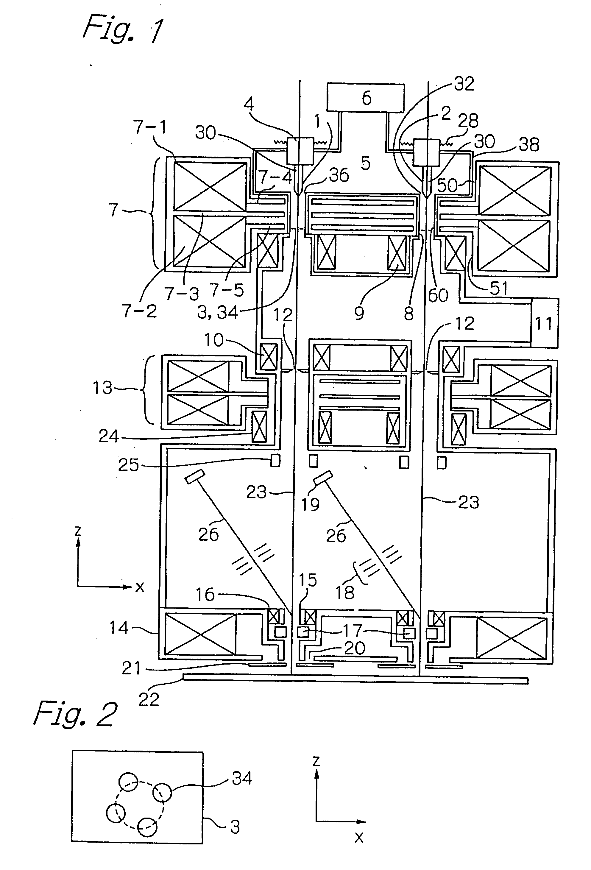
[0311] An electron beam apparatus according to an embodiment of the present invention as shown in FIG. 1 comprises an electron beam emitter section 32 having an electron gun 30, a plurality of apertures 34 disposed at a location out of an optical axis 23 and an electromagnetic lens 7 operable to control an on-axis electron beam and a plurality of off-axis electron beams emitted from the electron gun 30 so that said plurality of off-axis electron beams may pass through the apertures 34.

[0312] The electron beam emitter section 32 comprises two electron guns 30 and a housing 38 serving for holding the electron guns 30 as well as defining an electron gun chamber 5, and an ion pump 6 for evacuating the electron gun chamber 5 to high vacuum is attached to the housing 38. Further, each of the electron guns 30 is connected with a mechanism 28 for activating the electron gun 30 mechan...

second example

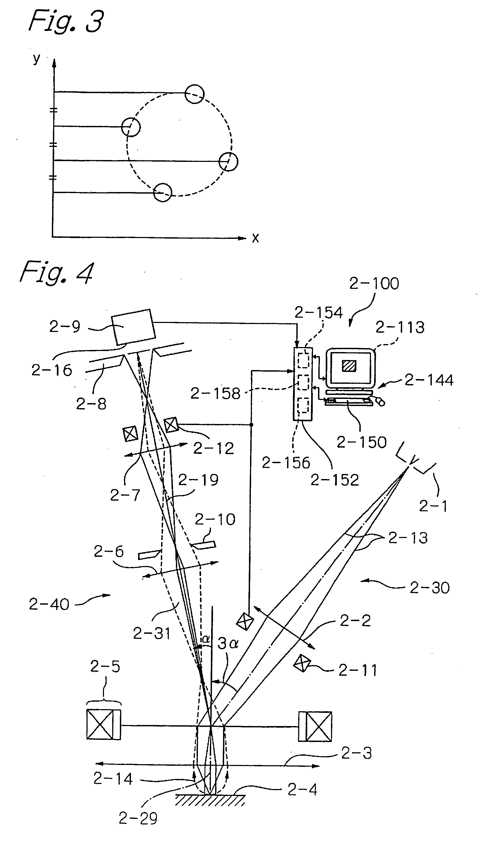
[0325] A first embodiment using a single beam embodying the second invention will now be described with reference to FIG. 4. An electron beam apparatus of this illustrated embodiment comprises an electron gun 2-1 serving as an electron beam source emitting a primary electron beam 2-13, a primary optical system 2-30 for guiding the primary electron beam onto a sample 2-4 to scan said sample 2-4 with the primary electron beam, a secondary electron detecting unit 2-9 having a detection surface 2-16 for detecting a secondary electron beam 2-14 emitting from the sample 2-4, a secondary optical system 2-40 for guiding the secondary electron beam 2-14 emitting from the sample 2-4 to be focused into an image on the detection surface 2-16 of the secondary electron detecting unit 2-9 and a controller 2-100 for controlling the electron beam apparatus.

[0326] The electron gun 2-1 of thermionic beam source type has been employed, in which electrons are emitted by heating an electron emission mat...

third example

[0346] An electron beam apparatus according to a second embodiment of the second invention will now be described with reference to FIG. 7. FIG. 7 is a schematic view of an electron beam apparatus according to the second embodiment of the present invention, in which a primary electron beam is composed of a multi-beam. This electron beam apparatus, as shown in FIG. 7(a), comprises an electron gun 2-41 serving as an electron beam source for emitting a primary electron beam, a primary optical system 2-42 for guiding the primary electron beam onto a sample 2-53 to scan the sample 2-53 with the primary electron beam, a secondary electron detecting unit 2-59 including a plurality of secondary electron beam detectors provided with detection surfaces 2-61 for detecting a secondary electron beam emanating from the sample 2-53, a secondary optical system 2-54 for guiding the secondary electron beam emitting from the sample 2-53 to be focused into an image on the detection surface 2-61 of the s...


PUM


Abstract

An object of the present invention is to provide an electron beam apparatus, in which a plurality of electron beams, e.g., four electron beams, is produced for one optical axis with a relatively high current achieved for each electron beam.
Provided is an electron beam apparatus comprising: an electron beam emitter (32) having an electron gun (30), said electron gun (30) disposed along an optical axis (23) and operable to emit a plurality of off-axis electron beams along a direction defined by a certain angle with respect to the optical axis (23); a plurality of apertures (34) disposed at a location offset from the optical axis (23); and an electromagnetic lens (7) for forming a magnetic field between the electron gun (30) and the apertures (34) to control the plurality of off-axis electron beams emitted from the electron gun (30) so that the plurality of off-axis electron beams passes through the apertures (34).

Description

BACKGROUND OF THE INVENTION [0001] The present invention relates to an electron beam apparatus allowing for an evaluation of a substrate as large as 8 inches or 12 inches with high precision (50 nm pixel to 25 nm pixel) as well as high throughput. Using a multi-beam is advantageous to achieve the high throughput, and an electron gun with a greater intensity of angular current is required to obtain the highly intensified multi-beam from a single electron gun, which may be represented by the electron gun of LaB6 and W hairpin having well-known angular current intensity values of 105 μA / Sr and 3.93×10⁶ μA / Sr, respectively. [0002] It can be seen from the comparison in the values of specific angular current intensity that the value of 104 μA / Sr for TaC is higher than 600 μA / Sr for ZrO / W but lower than 3.93×10⁶ μA / sr for the W hairpin. The electron gun of TaC, however, emits intensive beams in the four different off-optical axial directions and this makes it easier to form the multi-beam....

Claims


Application Information

Patent Timeline
IPC IPC(8): G01N23/225H01J37/28H01L21/66
CPCG01N23/225H01J2237/2817H01J2237/0635H01J37/28
Inventor NAKASUJI, MAMORUSATAKE, TOHRUNOJI, NOBUHARUMURAKAMI, TAKESHIWATANABE, KENJIKIMBA, TOSHIFUMISUEMATSU, KENICHI
Owner EBARA CORP
Why Eureka
Try Eureka