

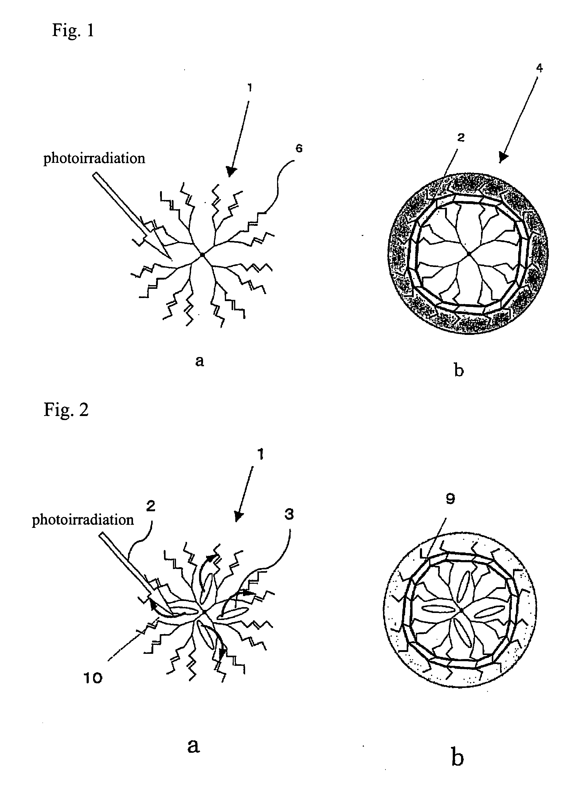
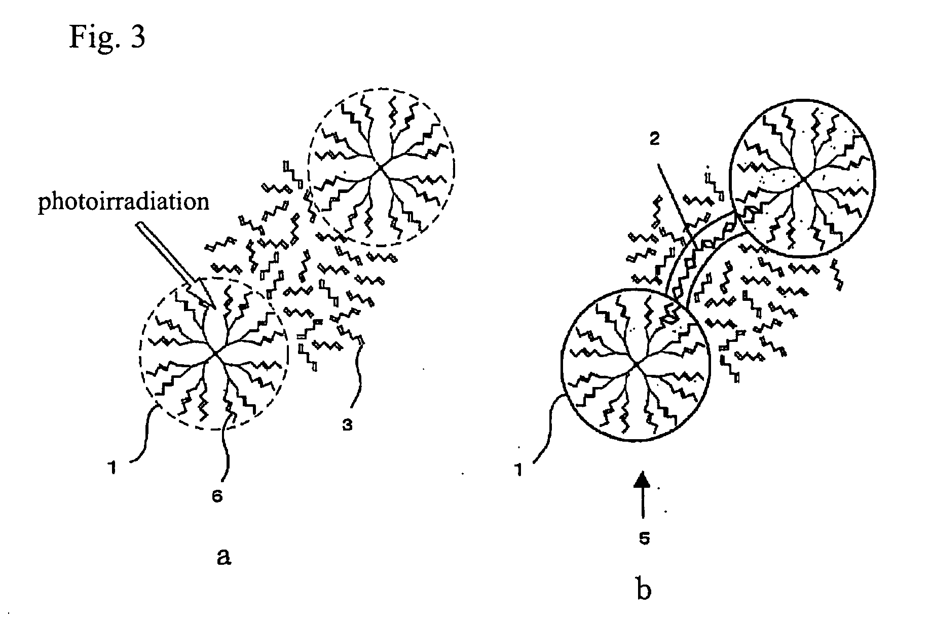
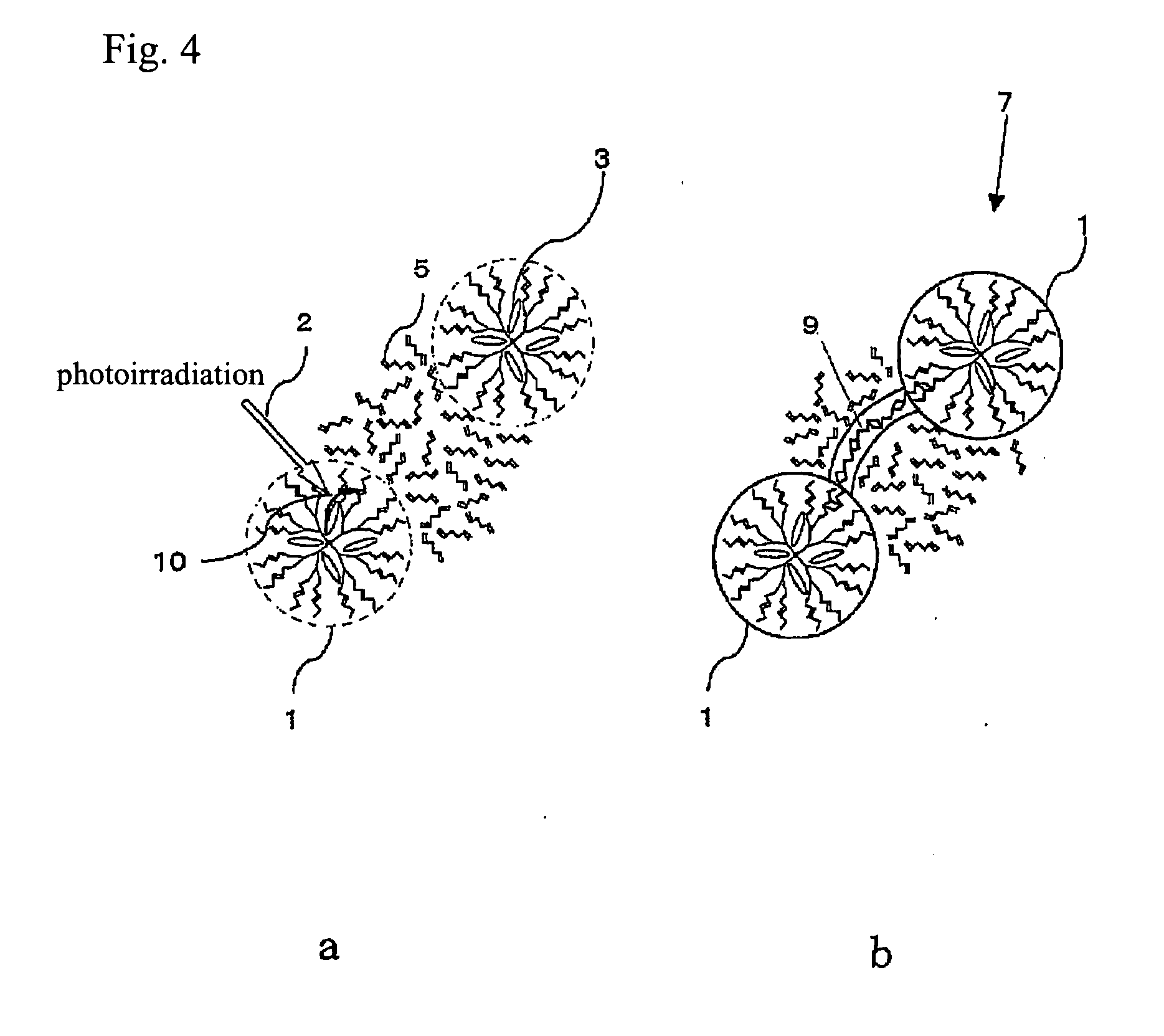
Process for production of molecular devices
a molecular aggregate and molecular technology, applied in the field of molecular aggregate production, can solve the problems of inability to work as element cannot achieve the effect of being a semiconductor no longer in principle, and achieve the effect of higher atomic density
- Summary
- Abstract
- Description
- Claims
- Application Information
AI Technical Summary
Benefits of technology
Problems solved by technology
Method used
Image

Examples
production example 1
Method of Synthesizing Dendrimer Having Cinnamic Acid
[0084] Amide Residue in Terminal Into a dichloromethane solution of a poly (propyleneimine) dendrimer (1.0 g, 3.2 mmol, made by Aldrich Corporation) of the first generation (n=1 in FIG. 8) containing a catalytic quantity of triethylamine, a solution of trans-cinnamyl chloride (0.63 g, 3.7 mmol, made by Aldrich Corporation) was dropped, and the resultant solution was stirred at 0° C. for one hour and then at room temperature for 40 hours. This reaction liquid was diluted with dichloromethane, was cleaned sequentially with ion-exchange water, an aqueous solution of sodium carbonate and an aqueous solution of sodium chloride, and was dried with magnesium sulfate. After filtration, dichloromethane was removed by an evaporator. The crude product was dialyzed and reprecipitated repetitively for three times, and was dried under a reduced pressure. Then, a white solid was obtained.
[0085] Each poly (propyleneimine) dendrimer of the third...
example 1
Production of Nano-Particle
Example 1-1
[0088] With the use of polypropylene imine dendrimer of the first generation (n=1) having residues of cinnamamide in the periphery of the molecular as shown in FIG. 8, the following experiment was carried out. A plurality of dichloromethane dilute solutions containing 3.0×10⁻⁵ (mol / L) of the dendrimer having cinnamamide by molar unit of cinnamamide in the dendrimer were prepared and were put in quartz cells having a dimension of 1.0 cm per side. The light having a wavelength of 313 nm which was taken out from a mercury xenon lamp having an output of 200 W, irradiated the previously prepared solution. With the photoirradiation, the absorption bands around 280 nm originated in the residue of cinnamamide decreased. The absorption spectrum after the photoirradiation was measured, and the abundance ratio of each trans isomer, cis isomer and associated body of the cinnamamide residue was calculated. The result is shown in Table 3. Here, the associat...
example 1-2
[0089] As in the Example 1-1 except that the polypropylene imine dendrimer of the third generation (n=3 in FIG. 8) was employed, an experiment was carried out. The result is shown in Table 3.
PUM
| Property | Measurement | Unit |
|---|---|---|
| Volume | aaaaa | aaaaa |
| Volume | aaaaa | aaaaa |
| Volume | aaaaa | aaaaa |
Abstract
Description
Claims
Application Information