Production method for light emitting element

a production method and light-emitting element technology, applied in the direction of polycrystalline material growth, crystal growth process, chemically reactive gas, etc., can solve the problems of increasing production costs, increasing production costs, and consuming a considerable amount of energy, so as to enhance the effect of introducing se or te, improving crystallinity of active layer, and enhancing binding tendency

Inactive Publication Date: 2005-10-13
SHIN-ETSU HANDOTAI CO LTD
View PDF5 Cites 20 Cited by
  • Summary
  • Abstract
  • Description
  • Claims
  • Application Information

AI Technical Summary

Benefits of technology

[0015] In the first invention, the p-type MgxZn1-xO layer grown by a metal organic vapor-phase epitaxy process is annealed in the oxygen-containing atmosphere during and / or after completion of the growth. This effectively prevents the oxygen deficiency from occurring, and successfully obtains a crystal having a less amount of n-type carrier. It is therefore no more necessary to add an excessive amount of p-type dopant for compensating the n-type carrier, and this makes it possible to obtain the light emitting device containing the p-type MgxZn1-xO layer, excellent in the stability, reproducibility and uniformity in the electrical characteristics.
[0061] To make MgaZn1-aO to have a p-type conductivity, it is necessary to add an appropriate p-type dopant as described in the above. As the p-type dopant, either one of, or two or more of N, Ga, Al, In, Li, Si, C, and Se are available. Among these, use of N is particularly preferable in view of obtaining desirable p-type characteristics. As the metal element dopant, either one of, or two or more of Ga, Al, In and Li are available, where Ga is particularly effective. Combined addition of these dopants with N can ensure desirable p-type characteristics in a more reliable manner.

Problems solved by technology

Use of the AlGaInN-base material, however, inevitably raises the costs because the material contains Ga and In as major components, both of which are relatively rare metals.
One of other major problems of the material is that the growth temperature thereof is as high as 700 to 1,000° C., and thus consumes a considerably large amount of energy for the production.
This is undesirable not only in terms of cost reduction, but also in terms of being against the stream of the times where discussions on energy saving and suppression of global warming are prevailing.
There is a problem that oxide layers of Zn and Mg are very likely to cause oxygen deficiency, and they inevitably tend to have an n-type conductivity, so that it is intrinsically difficult to obtain the crystal having only a less amount of n-type carrier (electrons) as a conductive carrier.
These oxide crystals, however, tend to have an n-type conductivity due to oxygen deficiency as described in the above, and it has long been believed as very difficult to form the p-type crystal or non-doped, semi-insulating crystal used for the active layer.
One possible method may be such as adding p-type dopant, but conversion of an n-type conductivity of a material into a p-type conductivity needs a large amount of dopants in order to compensate the whole portion of the existing n-type carriers and to excessively generate p-type carriers, so that problems in stability, reproducibility and uniformity of the electric characteristics remain unsolved.
Even for the case where the light emitting device is to be fabricated by a vapor-phase epitaxy process using any compound semiconductors other than the oxides of Zn and Mg (referred to as ZnO-base oxide or MgZnO-base oxide, hereinafter), only a tiny crystal defect ascribable to variation in reaction efficiency of the source gases may cause failure especially in the aforementioned InAIAsP / InGaAsP compound semiconductor laser, for which a very high level of quality is required, and may considerably lower the production yield.
The MBE process, however, cannot readily suppress generation of the oxygen deficiency due to its low pressure in the growth atmosphere, so that it is very difficult for the process to form the ZnO-base oxide layer which is indispensable for composing the light emitting device.
In the MOVPE process generally proceeded in a continuous manner, even if any accidental irregularity such as deficiency or dislocation of the atoms should occur, the layer growth for the next layer and thereafter continuously proceed while leaving the irregularity unrepaired, so that the process could not always ensure a desirable quality of the buffer layer which governs the crystal quality of the light emitting layer portion, and this has consequently been making it difficult to obtain the device having an excellent light emission efficiency.
The MgZnO-type oxide can be formed by the MOVPE process or MBE process as described in the above, but the formation process thereof is highly causative of oxygen deficiency of the MgZnO-type oxide and can readily result in degradation of crystallinity of the active layer composed of ZnO.
This consequently expands total half value width of the emission wavelength range ascribable to the active layer, reduces the emission intensity, and suppresses the emission efficiency for specific wavelength to be desired.

Method used


Image

  • Production method for light emitting element
  • Production method for light emitting element
  • Production method for light emitting element

Examples


embodiment 1

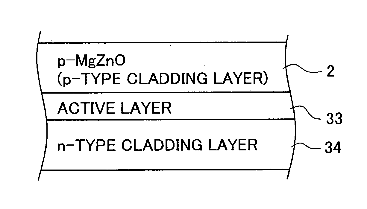
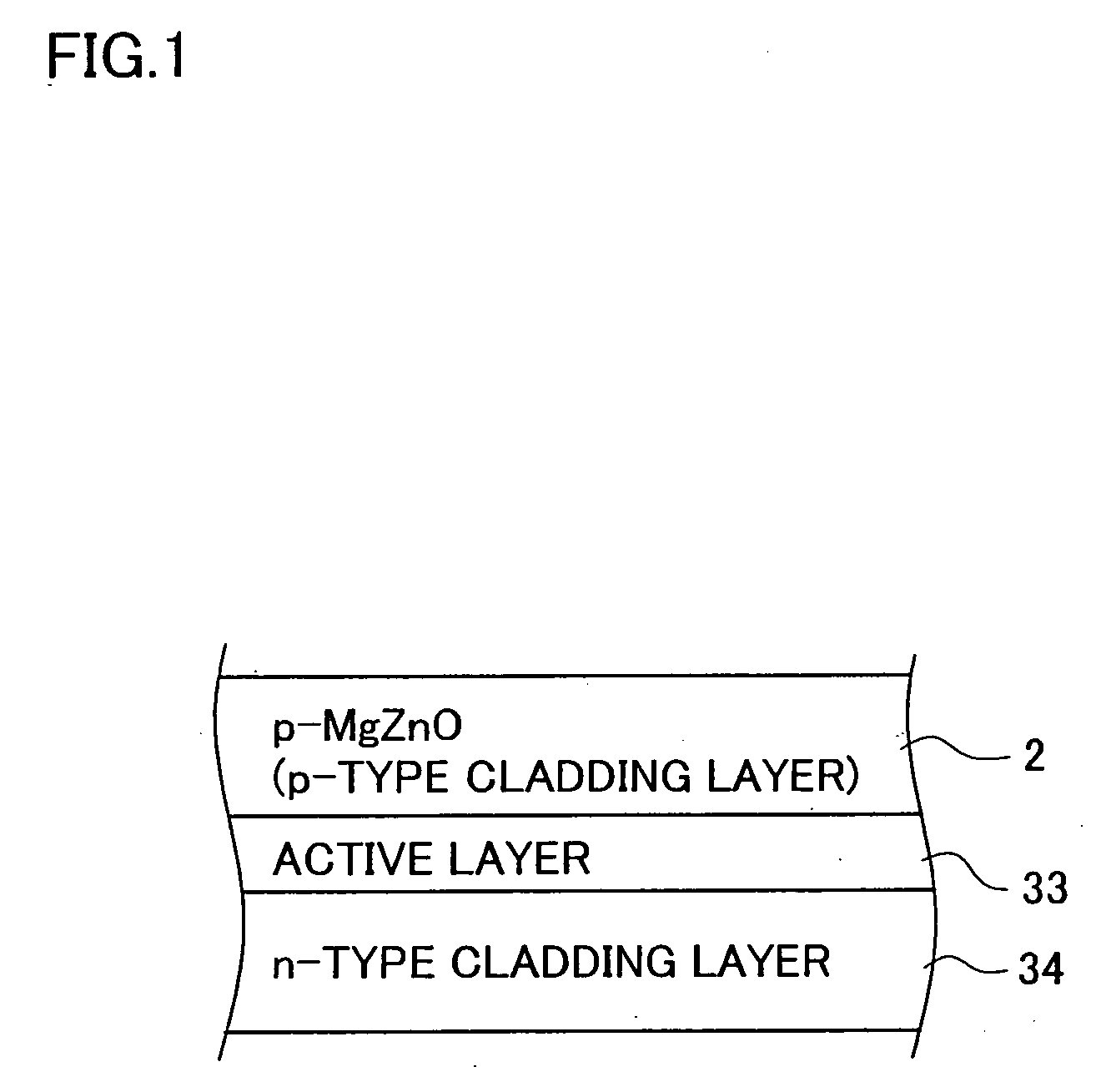
[0107]FIG. 1 is a drawing schematically showing a stacked structure of the essential portion of the light emitting device of the first invention, and the device has a light emitting layer portion in which an n-type cladding layer 34, an active layer 33 and a p-type cladding layer 2 are stacked in this order. The p-type cladding layer 2 is composed as a p-type MgxZn1-xO layer (0≦x≦1: may occasionally be referred to as p-type MgZnO layer 2, hereinafter). In the p-type MgZnO layer 2, a trace amount of either one of, or two or more of N, Ga, Al, In and Li, for example, are contained as a p-type dopant. The p-type carrier-concentration is adjusted within a range from 1×10¹⁶sites / cm3 to 8×10¹⁸ sites / cm3 as described in the above, and more specifically within a range from 1017 sites / cm3 to 1018 sites / cm3 or around.

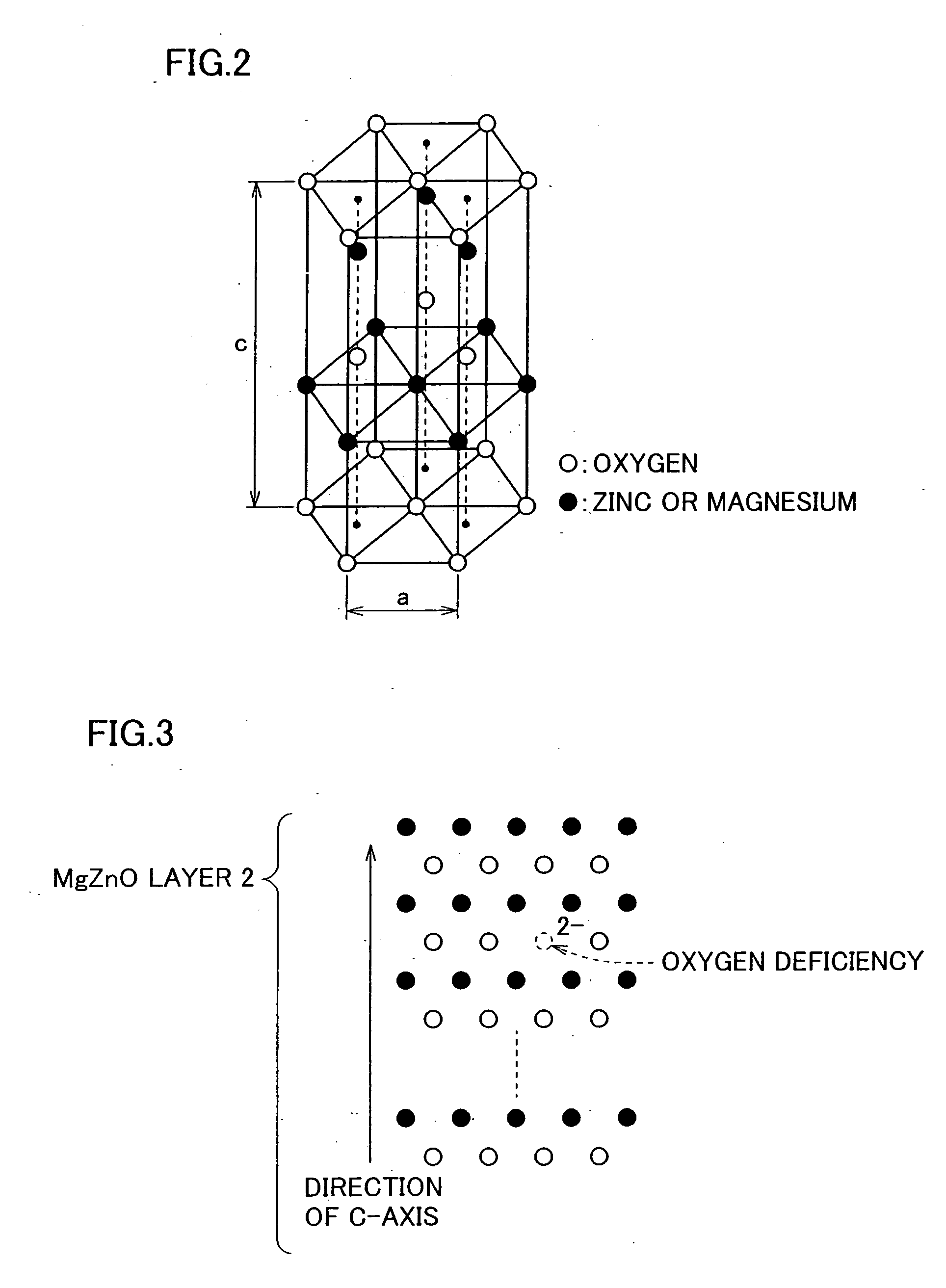
[0108]FIG. 2 is a schematic drawing of a crystal structure of MgZnO, where so-called wurtzite structure is shown. In this structure, oxygen-ion-packed planes and metal-ion (Zn i...

embodiment 2

[0150] The next paragraphs will describe an embodiment of the second invention. Since the essential portion of the light emitting device to which the second invention is applicable is same as described in Embodiment 1, detailed description will be omitted (see FIGS. 1 to 4, and FIGS. 10A and 10B). As shown in (a) of FIG. 6, the GaN buffer layer 11 is epitaxially grown again on the sapphire substrate 10, and further thereon the p-type MgZnO layer 52 (typically of 50 nm thick), the MgZnO active layer 53 (typically of 30 nm thick) and the n-type MgZnO layer 54 (typically of 50 nm thick) are formed in this order (inverted order of the growth also acceptable). The epitaxial growth of the individual layers in this embodiment can be carried out by the MOVPE process similarly to as described in Embodiment 1, where differences reside in the following points. More specifically, in the growth of the MgZnO active layer 53 and p-type MgZnO layer 52 herein, a ultraviolet lamp (e.g., excimer ultra...

embodiment 3

[0158] The next paragraphs will describe an embodiment of the third invention. Although the essential portion of the light emitting device to which the third invention is applicable is almost the same as described in Embodiment 1 (see FIGS. 1 to 5A, and FIGS. 10A and 10B), it is essential in the third invention to form the buffer layer as described below. That is, the buffer layer has the c-axis of the wurtzite crystal structure oriented to the thickness-wise direction, has a single metal atom layer as a metal monoatomic layer formed in contact with the substrate, and has the residual oxygen atom layers and metal atom layers alternatively stacked successive to the metal monoatomic layer. An exemplary fabrication process will be explained below.

[0159] First as shown in FIG. 13, a buffer layer 111 composed of MgZnO is epitaxially grown on the sapphire substrate 10, and further thereon an n-type MgZnO layer 34 (typically of 50 nm thick), an MgZnO active layer 33 (typically of 30 nm th...


PUM

PropertyMeasurementUnit
temperatureaaaaaaaaaa
band gap energyaaaaaaaaaa

Abstract

In a first invention, a p-type MgxZn1-xO-type layer is grown based on a metal organic vapor-phase epitaxy process by supplying organometallic gases which serves as a metal source, an oxygen component source gas and a p-type dopant gas into a reaction vessel. During and / or after completion of the growth of the p-type MgxZn1-xO-type layer, the MgxZn1-xO-type thereof is annealed in an oxygen-containing atmosphere. This is successful in forming the layer of p-type oxide in a highly reproducible and stable manner for use in light emitting device having the layer of p-type oxide of Zn and Mg. In a second invention, a semiconductor layer which composes the light emitting layer portion is grown by introducing source gases in a reaction vessel having the substrate housed therein, and by depositing a semiconductor material produced by chemical reactions of the source gas on the main surface of the substrate. A vapor-phase epitaxy process of the semiconductor layer is proceed while irradiating ultraviolet light to the main surface of the substrate and the source gases. This is successful in sharply enhancing reaction efficiency of the source gases when the semiconductor layer for composing the light emitting layer portion is formed by a vapor-phase epitaxy process, and in readily obtaining the semiconductor layer having only a less amount of crystal defects. In a third invention, a buffer layer having at least an MgaZn1-aO-type oxide layer on the contact side with the light emitting layer portion is grown on the substrate, and the light emitting layer portion is grown on the buffer layer. The buffer layer is oriented so as to align the c-axis thereof to the thickness-wise direction, and is obtained by forming a metal monoatomic layer on the substrate based on the atomic layer epitaxy, and then by growing residual oxygen atom layers and the metal atom layers. This is successful in obtaining the light emitting portion with an excellent quality. In a fourth invention, a ZnO-base semiconductor active layer included in a double heterostructured, light emitting layer portion is formed using a ZnO-base semiconductor mainly composed of ZnO containing Se or Te, so as to introduce Se or Te, the elements in the same Group with oxygen, into oxygen deficiency sites in the ZnO crystal possibly produced during the formation process of the active layer, to thereby improve crystallinity of the active layer. Introduction of Se or Te shifts the emission wavelength obtainable from the active layer towards longer wavelength regions as compared with the active layer composed of ZnO having a band gap energy causative of shorter wavelength light than blue light. This is contributive to realization of blue-light emitting devices.

Description

TECHNICAL FIELD [0001] This invention relates to a light emitting device and a method of fabricating the same. BACKGROUND ART [0002] There have long been demands for high-luminance, light emitting device capable of causing short-wavelength emission in the blue light region. Such light emitting device has recently been realized by using AlGaInN-base materials. Rapid progress has also been made in applying the device to full-color, light emitting apparatuses or to display apparatuses by combining it with red and green high-luminance, light emitting devices. Use of the AlGaInN-base material, however, inevitably raises the costs because the material contains Ga and In as major components, both of which are relatively rare metals. One of other major problems of the material is that the growth temperature thereof is as high as 700 to 1,000° C., and thus consumes a considerably large amount of energy for the production. This is undesirable not only in terms of cost reduction, but also in t...

Claims


Application Information

Patent Timeline
Patent Type & Authority Applications(United States)
IPC IPC(8): H01L21/365C30B25/18C23C16/40H01L33/00C30B25/02C30B25/10
CPCC23C16/40C30B25/02C30B25/105C30B25/183H01L33/0083C30B29/16H01L21/0242H01L21/02472H01L21/02477H01L21/0248H01L21/02483H01L21/02507H01L21/02554H01L21/02565H01L21/02579H01L21/0262
Inventor ISHIZAKI, JUN-YA
Owner SHIN-ETSU HANDOTAI CO LTD
Why Eureka
Try Eureka