Slim spacer device and manufacturing method

a spacer and manufacturing method technology, applied in semiconductor devices, semiconductor/solid-state device details, electrical apparatus, etc., can solve the problems of reducing the degree of lowering, increasing reducing the drive current, so as to reduce the width of the spacer, improve the mobility of charge, and reduce the s/d electrical resistance

Active Publication Date: 2005-10-13
TAIWAN SEMICON MFG CO LTD
View PDF6 Cites 43 Cited by
  • Summary
  • Abstract
  • Description
  • Claims
  • Application Information

AI Technical Summary

Benefits of technology

[0009] To achieve the foregoing and other objects, and in accordance with the purposes of the present invention, as embodied and broadly described herein, the present invention provides a CMOS structure comprising a Slim spacer and method for forming the same to reduce an S/D electrical resistance and improve charge mobility in a channel region.
[0010] In a first embodiment, the method includes providing a semiconductor substrate including a polysilicon or metal gate structure including at least one overlying hardmask layer; forming spacers selected from the group consisting of oxide/nitride and oxide/nitride oxide layers adjacent the polysilicon

Problems solved by technology

One problem with reducing junction depth is the effect of increasing the S/D region sheet resistance, which reduces drive current (ID).
Therefore, while it may be desirable to have a desired spacer width and a desired underlying SDE region width, the spacer width limits the degree of lowering the sheet resistance of the S/D region by salicide formation leading to lower drive current (ID).
In addition, as gate lengths become smaller, for example less than about 80 nanometers, conventional processes for forming spacers are no longer adequate to precisely position the S/D implant

Method used


Image

  • Slim spacer device and manufacturing method
  • Slim spacer device and manufacturing method
  • Slim spacer device and manufacturing method

Examples


Embodiment Construction

[0017] Although the method of the present invention is explained by reference to exemplary device sizes and is most advantageously used with preferred devices sizes, including spacer widths and gate lengths, it will be appreciated that the method of the present invention may be used with other device sizes as well.

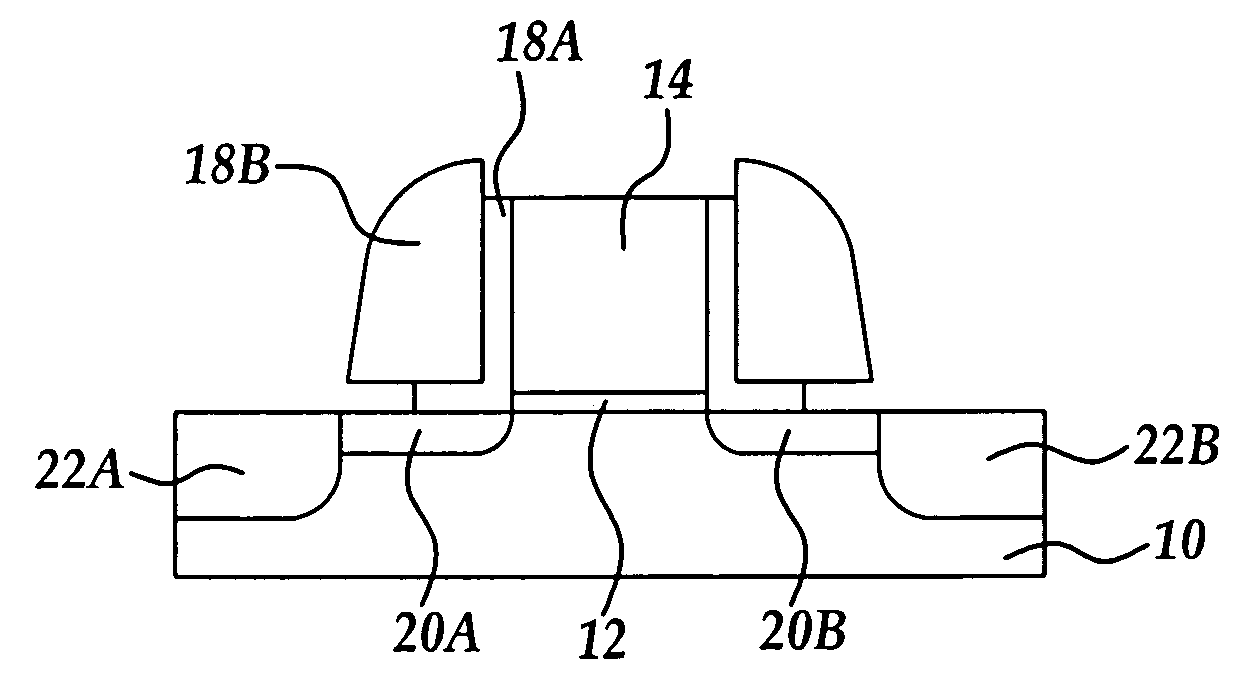
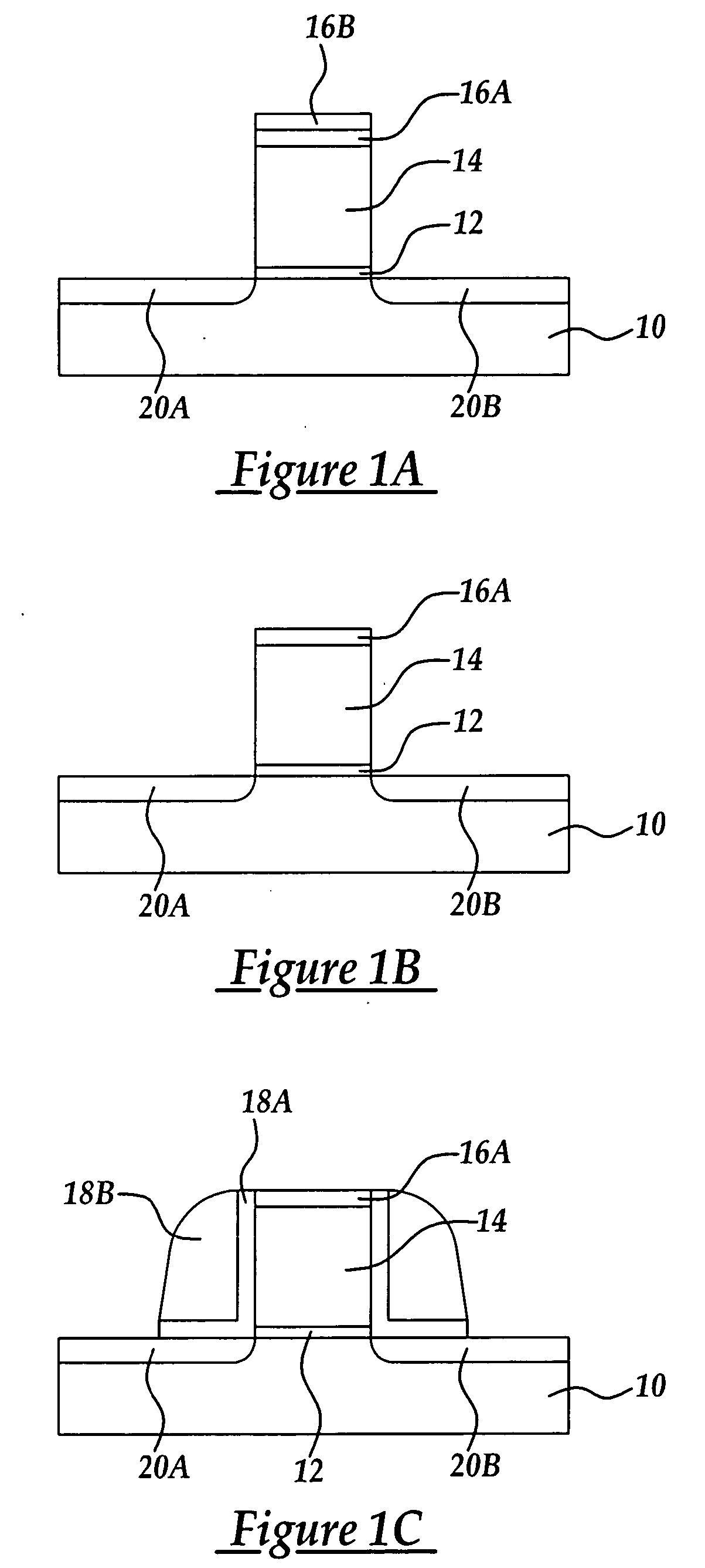
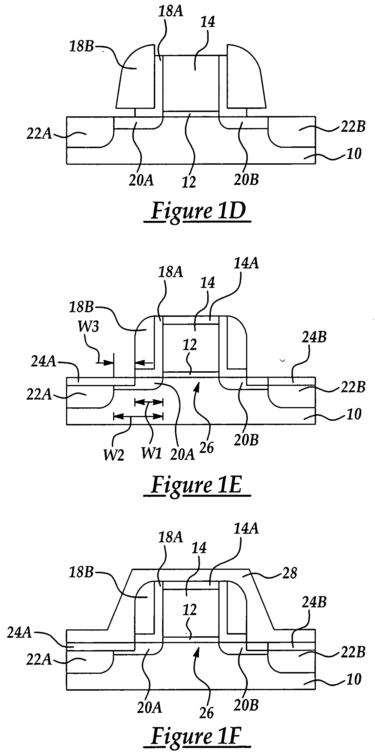
[0018] Referring to FIGS. 1A-1F is shown an exemplary implementation of the method of the present invention. Shown are a silicon or silicon germanium substrate 10, an overlying gate dielectric layer (such as oxide) portion 12, and an overlying polysilicon or metal gate electrode portion 14. In an aspect of the invention, at least one hardmask layers are deposited over a polysilicon or metal layer prior to forming the gate structure to form hardmask layer portions 16A and 16B overlying gate electrode portion 14 by conventional deposition, photolithographic and etching processes. For example the lowermost hardmask layer 16A is preferably formed of silicon oxide, e.g., LPCVD...


PUM


Abstract

A CMOS structure including a Slim spacer and method for forming the same to reduce an S/D electrical resistance and improve charge mobility in a channel region, the method including providing a semiconductor substrate including a polysilicon gate structure including at least one overlying hardmask layer; forming spacers selected from the group consisting of oxide/nitride and oxide/nitride oxide layers adjacent the polysilicon gate structure; removing the at least one overlying hardmask layer to expose the polysilicon gate structure; carrying out an ion implant process; carrying out at least one of a wet and dry etching process to reduce the width of the spacers; and, forming at least one dielectric layer over the polysilicon gate structure and spacers in one of tensile and compressive stress.

Description

FIELD OF THE INVENTION [0001] This invention generally relates to processes for forming semiconductor devices including CMOS and MOSFET devices and more particularly to a CMOS device and method for forming the same having a Slim spacer with improved electrical performance including reduced short channel effects and increased charge carrier mobility. BACKGROUND OF THE INVENTION [0002] As MOSFET and CMOS device characteristic sizes are scaled below 0.25 microns including below 0.1 micron, the device designs need to be modified for each generation of device scaling down. For example, short channel effects (SCE) are one of the most important challenges for designers to overcome as device critical dimensions are scaled down. Among the many manifestations of SCE, are Voltage threshold (VT) rolloff, drain induced barrier lowering (DIBL), and subthreshold swing variation. [0003] Source / Drain (S / D) junction depth and channel doping are some of the few parameters that can be changed to reduce...

Claims


Application Information

Patent Timeline
IPC IPC(8): H01L21/324H01L21/336H01L21/8242H01L29/78
CPCH01L21/324H01L29/665H01L29/6653H01L29/6656H01L29/6659H01L29/7833H01L29/7842H01L29/7843
Inventor HUANG, CHIEN-CHAOCHUNG, TONE-XUANYANG, FU-LIANG
Owner TAIWAN SEMICON MFG CO LTD
Why Eureka
Try Eureka