Implantation of deuterium in MOS and DRAM devices

a technology of mos and dram, which is applied in the direction of semiconductor devices, basic electric elements, electrical apparatus, etc., can solve the problems of reducing channel conductance, affecting the charge transport characteristics of semiconductor devices, and shifting threshold voltage, so as to improve the performance and reliability of mosfet devices

a technology of mos and dram, which is applied in the direction of semiconductor devices, basic electric elements, electrical apparatus, etc., can solve the problems of reducing channel conductance, affecting the charge transport characteristics of semiconductor devices, and shifting threshold voltage, so as to improve the performance and reliability of mosfet devices

US20050255684A1Inactive Publication Date: 2005-11-17PDF SOLUTIONS INC

Image

  • Implantation of deuterium in MOS and DRAM devices
  • Implantation of deuterium in MOS and DRAM devices
  • Implantation of deuterium in MOS and DRAM devices

Examples


Embodiment Construction

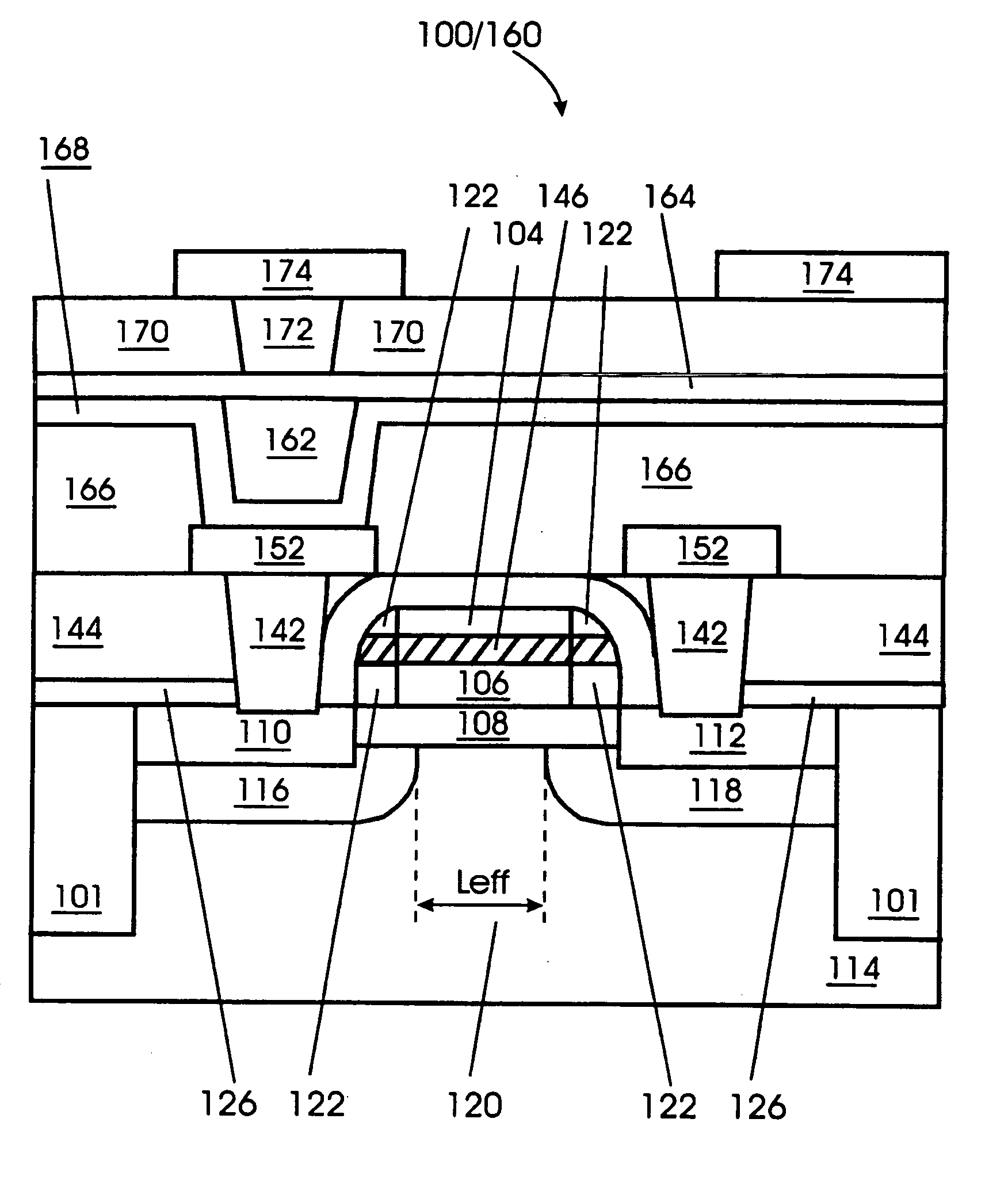
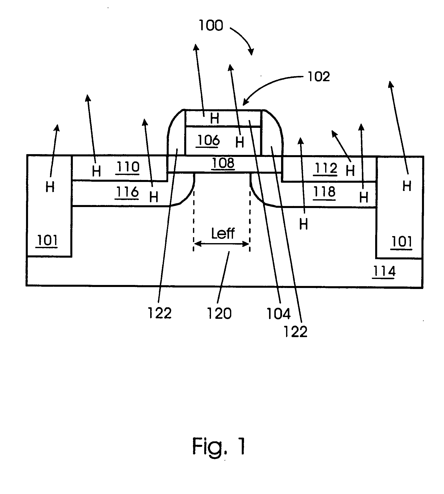
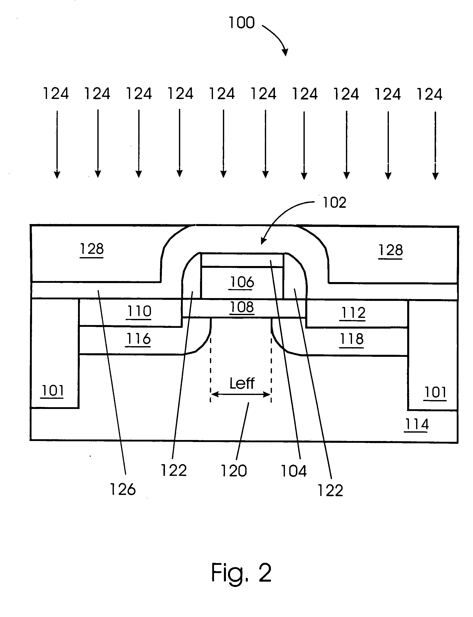
[0036] Referring to the Figures by characters of reference, FIG. 1 illustrates a Metal Oxide Semiconductor Field Effect Transistor (MOSFET) structure at the process stage where the formation of the spacer 122 has been completed. Shallow Trench Isolation (STI) 101 is used to isolate MOSFET 100 from other devices. STI 101 is typically composed of a dielectric material, such as SiO2. MOSFET 100 is formed having a gate stack 102 that includes a gate silicide 104, a poly-silicon gate 106, and a gate dielectric 108. Heavily doped source-drain regions 110 and 112 are formed in substrate 114 adjacent to gate stack 102. Lightly doped source-drain regions 116 and 118 are illustrated below source-drain regions 110 and 112. Between source-drain regions 110 and 112 lies channel 120 formed by applying a voltage across gate stack 102. An exemplary material for substrate 114 is silicon. An exemplary material for gate dielectric 108 is SiO2. Other materials for substrate 114 and gate dielectric 108 ...


PUM


Abstract

A structure and method passivates dangling silicon bonds by the introduction of deuterium into a Metal Oxide Semiconductor Field Effect Transistor (MOSFET) by ion implantation. The process of implantation provides precise placement of deuterium at optimum locations within the gate stack to create stable silicon-deuterium bond terminations at the Si—SiO2 interface within the gate-channel region. The deuterium is encapsulated in the MOSFET by the use of a Silicon Nitride (SiN) barrier mask. The ability of deuterium to passivate dangling silicon bonds is maximized by removing hydrogen present in the MOSFET and by use of an absorption layer to create a deuterium rich region.

Description

FIELD OF THE INVENTION [0001] The present invention relates to the field of semiconductor devices, and in particular to the use of deuterium to enhance the performance and reliability of semiconductor devices. BACKGROUND OF THE INVENTION [0002] New solutions for addressing the non-idealities present in semiconductor devices allows for continued reductions in scale and increases in performance. One of these non-idealities is interfacial traps, also referred to as surface states or interface states. Interfacial traps have wide-ranging and degrading effects upon the operational behavior of Metal-Oxide-Semiconductor (MOS) devices. Interfacial traps are allowed energy states in which electrons are localized in the vicinity of a material's surface. Interfacial traps primarily arise from unsatisfied chemical bonds that occur at the semiconductor-oxide interface. When a silicon lattice is abruptly terminated along a given plane to form a surface, one of the four surface-atom bonds is left d...

Claims


Application Information

Patent Timeline
17 Nov 2005
Publication
US20050255684A1
IPC
H01L21/265; H01L21/28; H01L21/30; H01L21/425; H01L21/8238; H01L29/78; H10B12/00
CPC
H01L21/265; H01L21/28176; H01L29/7833; H01L21/823814; H01L27/10873; H01L21/3003; H10B12/05
Inventors
KOLDIAEV, VIKTOR; BABOCK, JEFF