Unlock instant, AI-driven research and patent intelligence for your innovation.

Method forming transparent conductive film, transparent conductive film, glass substrate including the same and photoelectric conversion device using that glass substrate

a technology of transparent conductive film and transparent conductive film, which is applied in the direction of coatings, layered products, chemistry apparatuses and processes, etc., can solve the problems of short circuit in the photoelectric conversion device, deformation of defects in the transparent conductive film, and slowing down the line speed of the glass ribbon, so as to achieve high photoelectric conversion efficiency, low absorption coefficient at 400 to 550 nm wavelength, and high carbon concentration

Inactive Publication Date: 2005-12-15
NIPPON SHEET GLASS CO LTD +1
View PDF4 Cites 6 Cited by
  • Summary
  • Abstract
  • Description
  • Claims
  • Application Information

AI Technical Summary

Benefits of technology

The present invention aims to provide a method for forming a transparent conductive film on a glass ribbon using chemical vapor deposition (CVD) without generating large crystal grains in the film. The method ensures low carbon concentration and low absorption at certain wavelengths. The resulting film has high photoelectric conversion efficiency and can be used in photoelectric conversion devices without causing short circuits. The method involves film deposition at a certain speed using a raw material gas containing an organic tin compound. The resulting film has a low absorption coefficient and a low ratio of carbon atoms to tin atoms. The invention also includes a glass substrate with the transparent conductive film formed thereon and a photoelectric conversion device comprising this glass substrate.

Problems solved by technology

However, fluorine is a functional component that reduces the resistance of the transparent conductive film, so that a certain amount needs to be included.
Now, when an inorganic tin raw material is used in a high-temperature reaction system, defects may be formed in the transparent conductive film.
However on the other hand, if giant crystal grains are formed in the surface of the transparent conductive film, then it becomes difficult to form the photoelectric conversion layer uniformly, and moreover, the giant crystal grains may penetrate the photoelectric conversion layer and reach the rear electrodes, causing a short circuit in the photoelectric conversion device.
As such a preventive means, it is conceivable to carry out the film deposition at a location where the temperature of the glass ribbon is lower, such as in the annealing furnace 13, or to set a lower concentration of the raw material gas, but if these means are employed, thermal relaxation after the film deposition becomes difficult, because the film deposition takes place after the glass has hardened, so that the bonding strength of the transparent conductive film may decrease or it may be necessary to slow down the line speed of the glass ribbon in order to deposit the transparent conductive film uniformly, which means that this approach is not necessarily advantageous in an actual industrial setting.

Method used


Image

  • Method forming transparent conductive film, transparent conductive film, glass substrate including the same and photoelectric conversion device using that glass substrate
  • Method forming transparent conductive film, transparent conductive film, glass substrate including the same and photoelectric conversion device using that glass substrate

Examples


working examples

[0039] The following is a more detailed description of the present invention with reference to working examples.

[0040] First, the following is an explanation of a method for measuring / calculating the absorption coefficient of the transparent conductive film, the component concentrations of carbon and fluorine etc. in the transparent conductive film, and the ratio between the number of tin atoms and the number of carbon atoms in the transparent conductive film.

Absorption Coefficient of the Transparent Conductive Film

[0041] Methylene iodide with a refractive index of 1.79 was applied onto the transparent conductive film formed on an undercoating thin film, and a cover glass (#7059 by Corning Inc.) of 1 mm thickness was placed directly thereon, thus fabricating a sample in which the scattering loss due to the surface roughness of the conductive film is eliminated. The transmittance and reflectance of these samples at 400 to 550 nm were measured with a spectrophotometer, and the abs...

working example 1

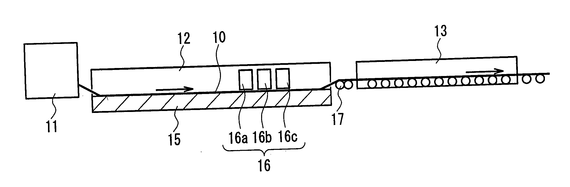
[0045] A gas mixture made of monosilane, ethylene, oxygen and nitrogen was supplied from the coater positioned furthest to the upstream side, and an undercoating film with about 30 nm film thickness whose principal component is silica was deposited on the glass ribbon. Subsequently, a gas mixture obtained by mixing a nitrogen carrier gas such that it contains 1.9 mol % dimethyltin dichloride (vapor), 36 mol % oxygen, 33 mol % water vapor, 5 mol % helium and 0.5 mol % hydrogen fluoride was supplied from a coater further downstream and a transparent conductive film of about 700 nm thickness whose principal component is tin oxide doped with fluorine was deposited at a film deposition speed of 5000 nm / min. The surface temperature of the glass ribbon just before depositing the transparent conductive film was about 650° C.

[0046] The film deposition conditions and the properties of this transparent conductive film are listed in Table 1 and Table 2.

working example 2

[0047] The concentration of the dimethyltin dichloride, the film deposition speed and the surface temperature of the glass ribbon just before depositing the transparent conductive film in Working Example 1 were changed as shown in Table 1, but otherwise the undercoating film and the transparent conductive film were deposited in the same manner as in Working Example 1.

[0048] The film deposition conditions and the properties of this transparent conductive film are listed in Table 1 and Table 2.


PUM

PropertyMeasurementUnit
absorption coefficientaaaaaaaaaa
glass transition temperatureaaaaaaaaaa
thicknessaaaaaaaaaa

Abstract

The present invention presents a method for forming a transparent conductive film whose principal component is tin oxide by so-called CVD on a glass ribbon, preventing the generation of giant crystal grains in the tin oxide, while ensuring that the concentration of carbon is low, or in other words, the absorption coefficient at 400 to 550 nm wavelength is low. In accordance with the invention, the method for forming a transparent conductive film whose principal component is tin oxide by CVD on a glass ribbon includes forming the transparent conductive film at a film deposition speed of 3000 to 7000 nm / min using a raw material gas including 0.5 to 2.0 mol % of an organic tin compound.

Description

TECHNICAL FIELD [0001] The present invention relates to methods for forming transparent conductive films that are used for photoelectric conversion devices, such as solar cells. Moreover, the present invention relates to glass substrates provided with a transparent conductive film formed with those methods, as well as photoelectric conversion devices using the same. BACKGROUND ART [0002] Many types of thin-film photoelectric conversion devices have been researched and developed, and in the most common configuration, a transparent conductive film whose principal component is tin oxide, a thin-film silicon layer serving as the photoelectric conversion layer, and a rear electrode made of aluminum are formed in that order on a transparent substrate, such as a glass sheet or the like. In this configuration, a transparent conductive film is desired that has a high transmittance of visible light, in order to guide more light to the photoelectric conversion layer, and that has a high conduc...

Claims


Application Information

Patent Timeline
Patent Type & Authority Applications(United States)
IPC IPC(8): C03C17/00C03C17/245C03C17/34C23C16/40C23C16/54H01L31/18
CPCC03C17/002C03C17/2453C03C17/3417C03C2217/211Y02E10/50C03C2218/152C23C16/407C23C16/545H01L31/1884C03C2217/213
Inventor FUJISAWA, AKIRAKIYOHARA, KOICHIROHIRATA, MASAHIROICHIKI, KIYOTAKASAWADA, TORU
Owner NIPPON SHEET GLASS CO LTD