Thin film semiconductor circuit, manufacturing method thereof, and image display apparatus utilizing the same thin film semiconductor circuit

Inactive Publication Date: 2006-01-05
HITACHI DISPLAYS
View PDF5 Cites 7 Cited by
  • Summary
  • Abstract
  • Description
  • Claims
  • Application Information

AI Technical Summary

Benefits of technology

[0017] According to the present invention, a thin film semiconductor circuit is provided, including thin film transistors, in which agglomeration generated when a high quality crystal is obtained with melting and re-crystallization can be controlle

Problems solved by technology

Meanwhile, in the case of forming a single crystal silicon film, the melting time of the silicon film becomes longer and agglomeration is generated.
However, if a structure which will become a trigger, such as fine particle, a non-uniform distribution of film thickness or a non-uniformed laser intensity, exists, agglomeration occurs.
Reduction of such a structure, which will become a trigger, may

Method used


Image

  • Thin film semiconductor circuit, manufacturing method thereof, and image display apparatus utilizing the same thin film semiconductor circuit
  • Thin film semiconductor circuit, manufacturing method thereof, and image display apparatus utilizing the same thin film semiconductor circuit
  • Thin film semiconductor circuit, manufacturing method thereof, and image display apparatus utilizing the same thin film semiconductor circuit

Examples


Example

[0041] First Embodiment

[0042] In the first embodiment, another element is substituted for the oxygen of the silicon oxide film. In this case, the polarization coefficient may be lowered when an element having an electronegativity which is smaller than that of the oxygen element, namely the element belonging to the group smaller than the 6A group, is substituted. Usually, the CVD film formed using TEOS (Tetraethoxysilane) gas as the raw material is employed as the silicon oxide film because it has excellent coverage.

[0043] An example of forming a TEOS film will be explained below. First, oxygen gas, helium gas, and TEOS gas are introduced into a chamber in which a substrate is prepared in the flow ratio of 1:1:1. After the gases are stabilized, plasma is generated with the RF output of 450 W in order to form an oxide film on the substrate using the chemical vapor deposition method. When the film is grown up to a thickness of 100 nm under a time control (7 seconds or more), the reac...

Example

[0051] Second Embodiment

[0052] Moreover, as a second embodiment, a film other than the silicon oxide, film which can improve wettability of the melted silicon, may be employed for the underlayer UCL. For example, it is recommended to employ silicon carbide (SiC) and diamond-like carbon (DLC) as the underlayer. Any method can be selected from the ion beam evaporation, sputtering, arc discharge and CVD methods for formation of SiC and DLC. DLC may also be formed as a semiconductor material depending on the film forming conditions. When the resistance value is lowered, a disadvantage occurs in that the element-to-element insulation becomes bad and a parasitic element, such as a thyristor, operates. However, as disclosed in the non-patent document 3 (Thin Solid Films 373 2000 pp251-254), the necessary insulation property can be acquired by lowering the film forming temperature and the RF output in regard to the resistivity of DLC.

[0053] For the method of manufacturing a semiconductor ...

Example

[0055] Third Embodiment

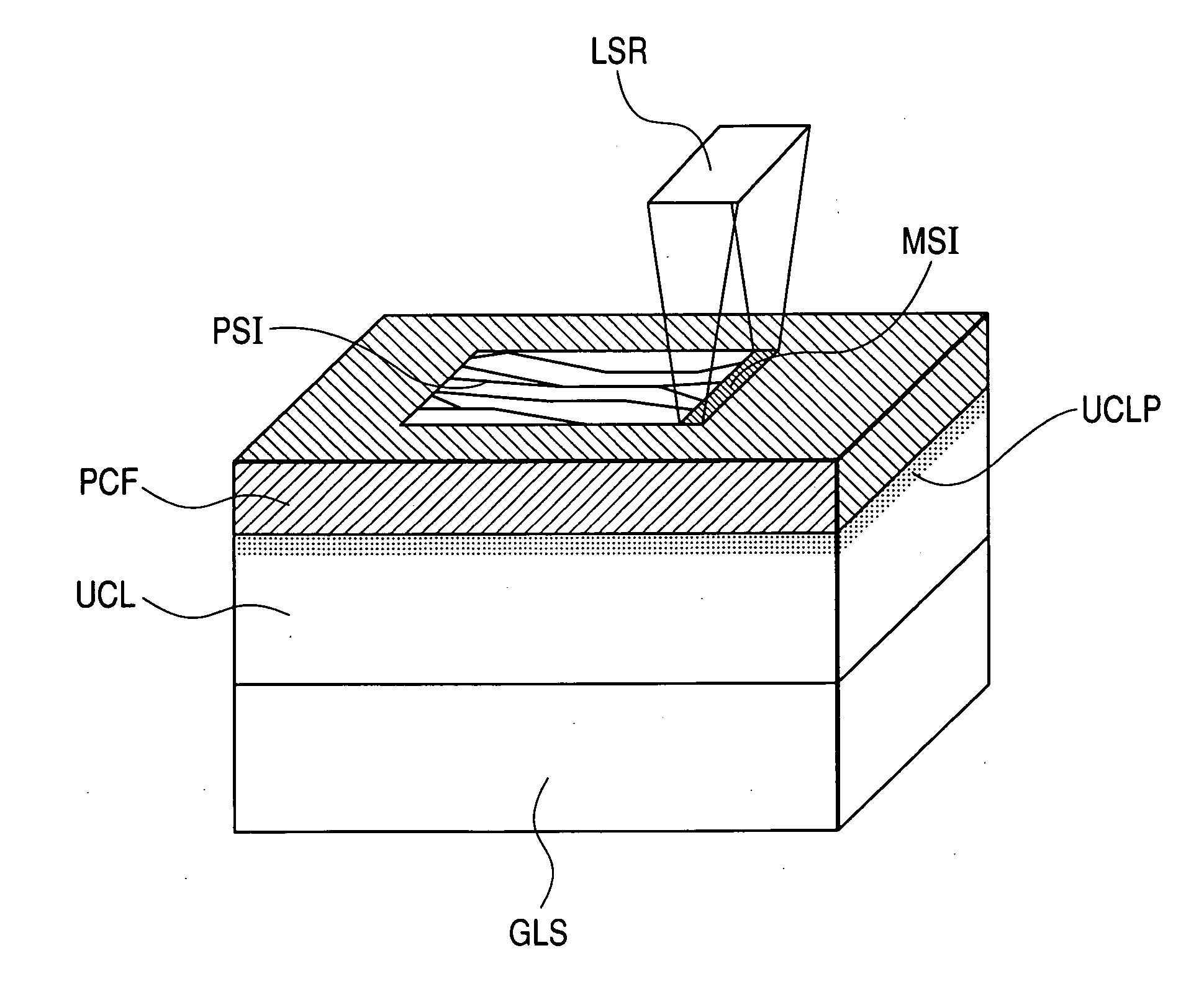
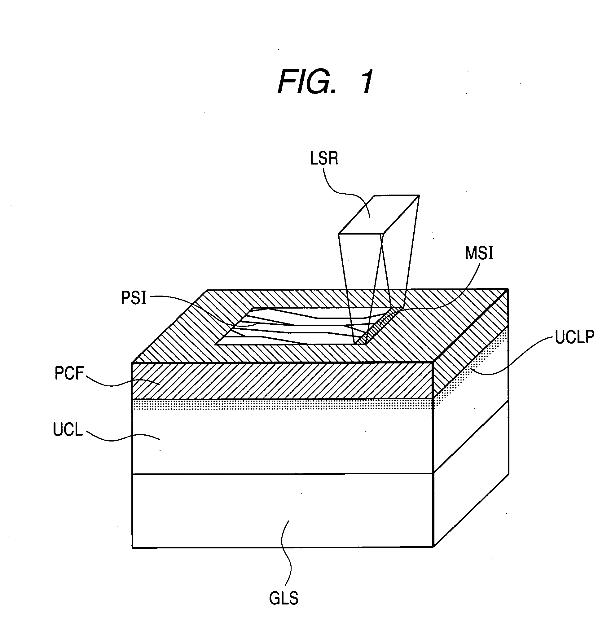
[0056] Unlike the ideal silicon oxide film, the actual silicon oxide film includes OH group and H2Omolecules in the film. These molecules are in the state captured with a hydrogen bond and a weak bond like an intermolecular force, and the amount of these molecules is determined depending on the film forming method and raw material gas or the like. When the SiO film is employed as the underlayer UCL, the amount of OH group and H2O molecules captured are considered to be larger than that of the TEOS film. With implementation of a high-temperature heat treatment, such as annealing in a furnace or annealing by excimer laser, an oxygen atom resulting from an OH group and H2O in the SiO film can be introduced into the silicon film PCF. Moreover, a similar effect can also be attained at the time of melting and re-crystallization using the laser beam LSR. As a result, the wettability of the melted silicon film MSI for the silicon oxide film can be improved, and agglo...


PUM


Abstract

Agglomeration of a polycrystalline silicon film is eliminated at the time of obtaining a high quality polycrystalline silicon film by forming a silicon layer on an insulating film substrate and conducting long-term melting and re-crystallization. For this purpose, a layer or a plurality of layers of an underlayer UCL are provided on an insulating substrate GLS, the area near the surface in contact with a precursory silicon film PCF provided on this underlayer UCL is formed as an insulating film UCLP showing a film composition to improve the wettability of the melted silicon layer, and thereafter a high quality polycrystalline silicon film PSI is formed through elimination of agglomeration by melting of the precursory silicon film PCF using a laser beam LSR.

Description

CLAIM OF PRIORITY [0001] The present application claims priority from Japanese application JP 2004-195150 filed on Jul. 1, 2004, the content of which is hereby incorporated by reference into this application. FIELD OF THE INVENTION [0002] The present invention relates in general to a thin film semiconductor circuit, a method of manufacture thereof, and an image display apparatus formed of such a thin film semiconductor circuit; and, more particularly, the present invention is suitable for providing a low temperature process polycrystalline silicon thin film transistor which is used to constitute the pixels, a driver circuit and, the other peripheral circuits of a flat type image display apparatus, such as a liquid crystal display device or an organic EL display device. [0003] A thin film transistor (polycrystalline silicon FET) in which the channel thereof is formed of polycrystalline silicon (poly-silicon) has been developed for the pixels and the driver circuit (driver) of such pi...

Claims


Application Information

Patent Timeline
IPC IPC(8): H01L29/745H01L21/335
CPCH01L27/12H01L27/3244H01L27/1285H01L29/78603H01L29/78675H01L29/04H10K59/12
Inventor TAI, MITSUHARUHATANO, MUTSUKOTAKAHARA, YOICHITAKAHASHI, HIROKIYAZAKI, AKIONODA, TAKESHI
Owner HITACHI DISPLAYS
Why Eureka
Try Eureka