Organic silica-based film, method of forming the same, composition for forming insulating film for semiconductor device, interconnect structure, and semiconductor device

a technology of organic silica and film, applied in the direction of liquid organic insulators, semiconductor/solid-state device details, transportation and packaging, etc., can solve the problems of damage to the transistor structure in the lsi, dehydration-condensation does not rapidly proceed, and accumulation of electric charges

Inactive Publication Date: 2006-01-12
JSR CORPORATIOON
View PDF15 Cites 54 Cited by
  • Summary
  • Abstract
  • Description
  • Claims
  • Application Information

AI Technical Summary

Problems solved by technology

However, since the reaction of the organic silica sol is a solid-phase reaction, dehydration-condensation does not rapidly proceed due to diffusion control.
On the other hand, accumulation of electric charge due to electron beam application may damage the transistor structure in the LSI.
A silica film cured by using a photoacid generator or a photobase generator generally exhibits high hygroscopicity due to a large amount of residual silanol.
However, this process does not achieve an improvement over the above-described silica film thermal curing method.
Moreover, a composition containing a photoacid generator or a photobase generator cannot satisfy the quality as an insulating film of an LSI semiconductor device for which high insulation reliability is demanded, since the photoacid generator, the photobase generator, or an acidic or basic substance generated by the photoacid generator or the photobase generator functions as a charge carrier to impair the insulating properties or causes an interconnect metal to deteriorate.
Therefore, this technology does not promote a crosslinking reaction of silica sol by ultraviolet radiation.
However, only a limited number of documents have been reported relating to a technology which uses ultraviolet radiation for curing organic silica sol in order to form an interlayer dielectric for an LSI semiconductor device.
However, while a silica film formed according to this technology has a high modulus of elasticity and high hardness due to an increase in the amount of the SiO2 bond, the moisture absorption and the dielectric constant are increased due to an increase in hydrophilicity of the film.
A film having high hygroscopicity generally tends to be damaged by reactive ion etching (RIE) performed in the processing of an interlayer dielectric of a semiconductor device, and exhibits insufficient chemical resistance against a wet cleaning liquid.
However, it is difficult to cause the crosslink site (silanol) of the component Q to completely react.
If the amount of component Q is increased to a large extent, the amount of residual silanol is increased after thermal curing, whereby the resulting film exhibits hydrophilicity and high hygroscopicity.
However, since the organic silica sol containing a large amount of component Q has a low molecular chain mobility due to high crosslink density, the diffusion barrier during the solid-phase reaction is considerably high.

Method used


Image

  • Organic silica-based film, method of forming the same, composition for forming insulating film for semiconductor device, interconnect structure, and semiconductor device
  • Organic silica-based film, method of forming the same, composition for forming insulating film for semiconductor device, interconnect structure, and semiconductor device

Examples


example 2

4.1.1b Example 2

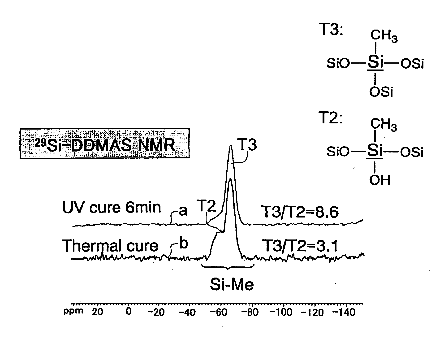
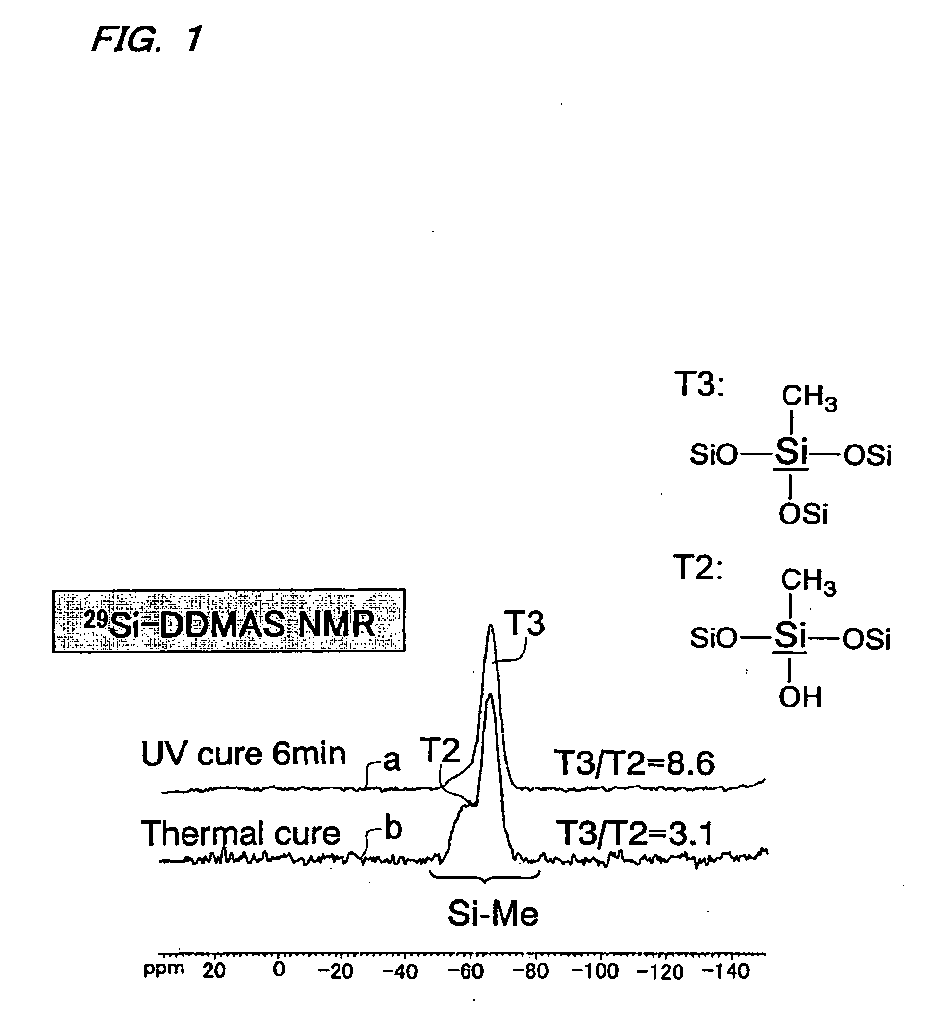
[0145] In a quartz flask equipped with a condenser, 41.2 g of tetramethoxysilane and 180.1 g of methyltrimethoxysilane were dissolved in 227.3 g of propylene glycol monoethyl ether. After the addition of 136.5 g of ion-exchanged water to the solution, the mixture was stirred for one hour. After the addition of a solution prepared by dissolving 0.106 g of tetrakis(acetylacetonate)titanium in 79.9 g of propylene glycol monoethyl ether, the mixture was allowed to react at 50° C. for three hours. After the addition of 887.4 g of propylene glycol monoethyl ether, the reaction solution was cooled to room temperature. The reaction solution was concentrated under reduced pressure until the solid content became 15%. After the addition of 35.0 g of acetylacetone, propylene glycol monoethyl ether was added so that the solid content became 10% to obtain a film forming composition 2. The organic silica sol included in the composition 2 had a carbon content of 14.1 mol %, a sodium...


PUM

PropertyMeasurementUnit
wavelengthaaaaaaaaaa
densityaaaaaaaaaa
relative dielectric constantaaaaaaaaaa

Abstract

A method of forming an organic silica-based film, including: applying a composition for forming an insulating film for a semiconductor device, which is cured by using heat and ultraviolet radiation, to a substrate to form a coating; heating the coating; and applying heat and ultraviolet radiation to the coating to effect a curing treatment, wherein the composition includes organic silica sol having a carbon content of 11.8 to 16.7 mol %, and an organic solvent, the organic silica sol being a hydrolysis-condensation product produced by hydrolysis and condensation of a silane compound selected from compounds shown by the general formulae (1): R1Si(OR2)3, (2): Si(OR3)4, (3): (R4)2Si(OR5)2, and (4): R6b(R7O)3-bSi—(R10)d—Si(OR8)3-cR9c.

Description

[0001] Japanese Patent Application No. 2004-203646, filed on Jul. 9, 2004, and Japanese Patent Application No. 2004-248578, filed on Aug. 27, 2004, are hereby incorporated by reference in their entirety. BACKGROUND OF THE INVENTION [0002] The present invention relates to an organic silica-based film, a method of forming the same, a composition for forming an insulating film for a semiconductor device, an interconnect structure, and a semiconductor device. [0003] A silica (SiO2) film formed by a vacuum process such as a CVD process has been widely used as an interlayer dielectric for a semiconductor device used in a large-scale integrated circuit (LSI) or the like. In recent years, in order to form an interlayer dielectric having a more uniform thickness, a spin-on-glass (SOG) film, which is a coating-type insulating film containing an alkoxysilane hydrolysate as the major component, has also been used. Along with an increase in the degree of integration of the LSI, a low-relative-di...

Claims


Application Information

Patent Timeline
Patent Type & Authority Applications(United States)
IPC IPC(8): H01B3/20H01L23/48H01L21/31C09D183/04H01L21/312
CPCC09D183/04C09D183/14H01L21/02126H01L21/3122H01L21/02282H01L21/02348H01L21/02216Y10T428/31663H01L21/31
Inventor TSUCHIYA, HAJIMEEGAWA, HIROMIKOKUBO, TERUKAZUSHIOTA, ATSUSHI
Owner JSR CORPORATIOON
Why Eureka
Try Eureka