
Thin film capacitor

a film capacitor and capacitor technology, applied in the direction of capacitors with voltage varied dielectrics, transistors, stereophonic arrangments, etc., can solve the problems of hysteresis, inconvenient voltage application, and inability to achieve the desired attenuation at low frequencies without sacrificing the band-pass, so as to minimize the insertion loss and phase characteristic variation, the effect of reducing the q factor resulting from voltage application

Active Publication Date: 2006-01-19
KYOCERA CORP
View PDF6 Cites 11 Cited by
  • Summary
  • Abstract
  • Description
  • Claims
  • Application Information

AI Technical Summary

Benefits of technology

[0015] The invention has been devised in view of the two problems stated hereinabove, and accordingly its first object is to provide a thin film capacitor which is so designed that, in a case of fabricating a band-pass filter therewith, a desired attenuation can be fulfilled without adjusting a circuit constant. A second object of the invention is to provide a variable capacitor in which Q factor reduction resulting from voltage application can be minimized at a predetermined frequency. Yet another object of the invention is to provide a variable filter or the like in which insertion loss and phase characteristic variation can be minimized successfully by using such a variable capacitor.
[0029] Hereinbelow, a description will be given as to a stacked-type variable capacitor having the advantage of relative easiness of setting, in which a piezoelectric oscillation takes place mainly in the thicknesswise longitudinal vibration mode. A fundamental wave f1 for this vibration mode is determined by the thickness of a high-dielectric-constant thin film; the film thicknesses of electrodes having sandwiched therebetween the high-dielectric-constant thin film; and the sonic velocity and acoustic impedance of a material in use. Assuming that t is the entire thickness of the structure constituting an oscillatory portion including the electrodes, and that V is the effective sonic velocity of a sonic wave propagating through the oscillatory portion, then f1 is given by: f1=V / 2t, while a higher-order resonant frequency fn is roughly given by: fn=nV / 2t (n=1, 3, 5 . . . ). The effective sonic velocity refers to the average of sonic velocities that differ according to materials used to form the individual layers, when viewed in the oscillatory portion as a whole. The material and film thickness are so determined that each of the resonant frequencies does not fall in the range of usable frequencies. The desired film thickness is determined by the usable frequency and the effective sonic velocity as seen in the oscillatory portion. The fundamental wave can be shifted to a high-frequency level by reducing the film thickness or by increasing the effective sonic velocity. It is preferable that the film thickness is so adjusted that the fundamental wave is beyond the range of usable frequencies. This makes it possible to avoid the influence of resonance on the Q factor at the time of voltage application. In this way, according to the invention, materials in use and film thickness are preferably so determined as to minimize Q factor reduction resulting from voltage application at a predetermined frequency.
[0030] Next, the setting of acoustic impedance will be explained. At an interface between layers of different acoustic impedances, part of an oscillatory wave is reflected, but the remainder thereof is transmitted therethrough. This results in occurrence of resonance for the reflected oscillatory wave and resonance for the transmitted oscillatory wave. Accordingly, in the setting of acoustic impedance, containment of vibrational energy is achieved in the pair of electrodes and the dielectric thin film, and acoustic isolation is effected in the other layers; wherefore unnecessary excitation can be avoided. In this way, according to the invention, the acoustic impedance of each of the materials and film thickness are so determined as to minimize Q factor reduction resulting from voltage application at a predetermined frequency. In the invention, the thin film capacitor preferably ranges in usable frequency from 1.7 to 2.1 GHz. This frequency range applies to cellular mobile phones, for example. It is thus preferable to see to it that Q factor reduction resulting from voltage application is avoided within the usable frequency range.
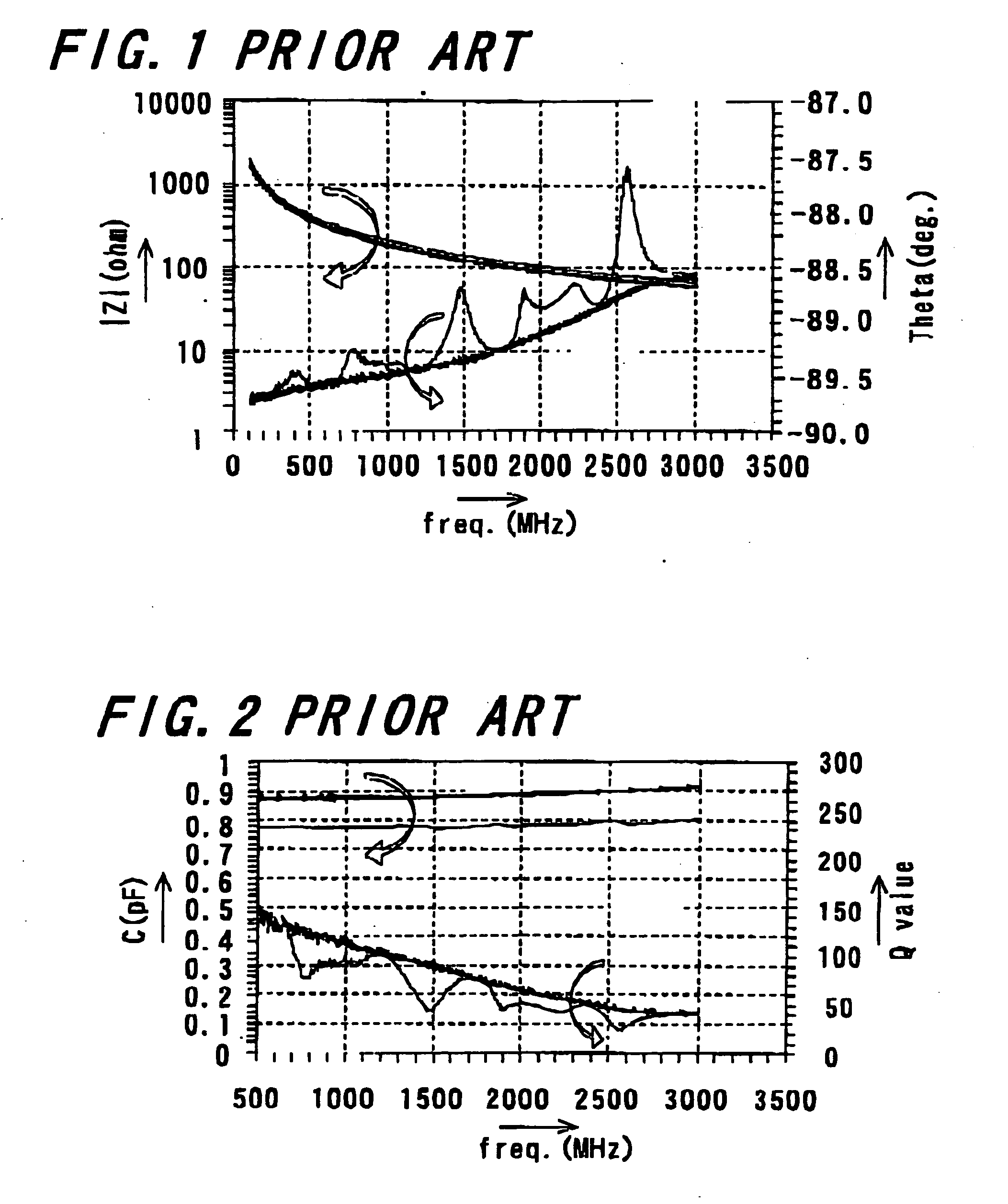
[0032] Moreover, in the invention, the signal frequency (usable frequency) is adjusted to fall in between the values representing the adjacent peaks of the impedance phase characteristic. This makes it possible to provide a thin film capacitor in which Q factor reduction resulting from voltage application can be minimized at a predetermined frequency. By using such a thin film capacitor, it is possible to realize a variable filter or the like with low insertion loss and little phase characteristic variation.
[0035] According to the invention, by using such dielectric layers, it is possible to realize a variable capacitor having a high dielectric constant, in which the dielectric constant may vary greatly by a voltage applied externally.
[0039] According to the invention, the pair of electrodes and the dielectric layer are mechanically protected by the protective layer from external perturbations. Besides, the protective layer gives protection against material degradation due to a chemical reaction with humidity or oxygen; contamination due to deposition of foreign objects such as dust; quality deterioration due to breakage caused by mounting; contamination due to a chemical agent or the like; and oxidation.

Problems solved by technology

The first problem is that, in fabricating a band-pass filter with use of a thin film capacitor in which the Q factor decreases monotonously with respect to frequencies as shown in FIG. 2, for example, a desired attenuation at low frequencies cannot be fulfilled without sacrificing the band-pass characteristic (Loss).
The second problem is associated with a case where a thin film capacitor employing a high-dielectric-constant thin film having the above-stated perovskite crystal structure is used as a variable capacitor.
When the material exhibits ferroelectricity, it is not suited for the variable capacitor.
Furthermore, the hysteresis corresponds to a lag behind a polarized alternating current, that is; a high dielectric loss.
However, there is a possibility that the ferroelectricity of BaTiO3 appears in an abated state in a paraelectric-ferroelectric phase boundary region, which may lead to slight capacitance hysteresis.
The piezoelectricity is intensified by a voltage applied to vary the capacitance, which may result in occurrence of resonance in the impedance's amplitude and phase characteristics.
The influence thereof will be problematic when it is notable within the range of usable frequencies set for the variable capacitor.
In a case where the variable capacitor in which the Q factor is greatly reduced after voltage application is employed as a constituent component for a filter, a resonator, or the like, inconveniently, a loss that the variable element incurs increases by voltage application.

Method used


Image

  • Thin film capacitor
  • Thin film capacitor
  • Thin film capacitor

Examples


example

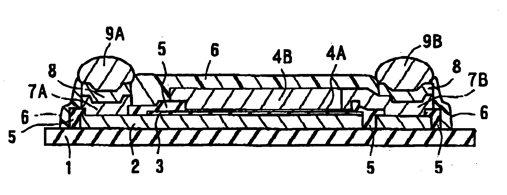
[0061] As an example embodying the invention, a variable capacitor was fabricated that is operable at a frequency of approximately 1.9 GHz. In order to avoid Q factor reduction resulting from resonance at the usable frequency of 1.9 GHz, layer configuration, materials, and film thickness were determined as follows.

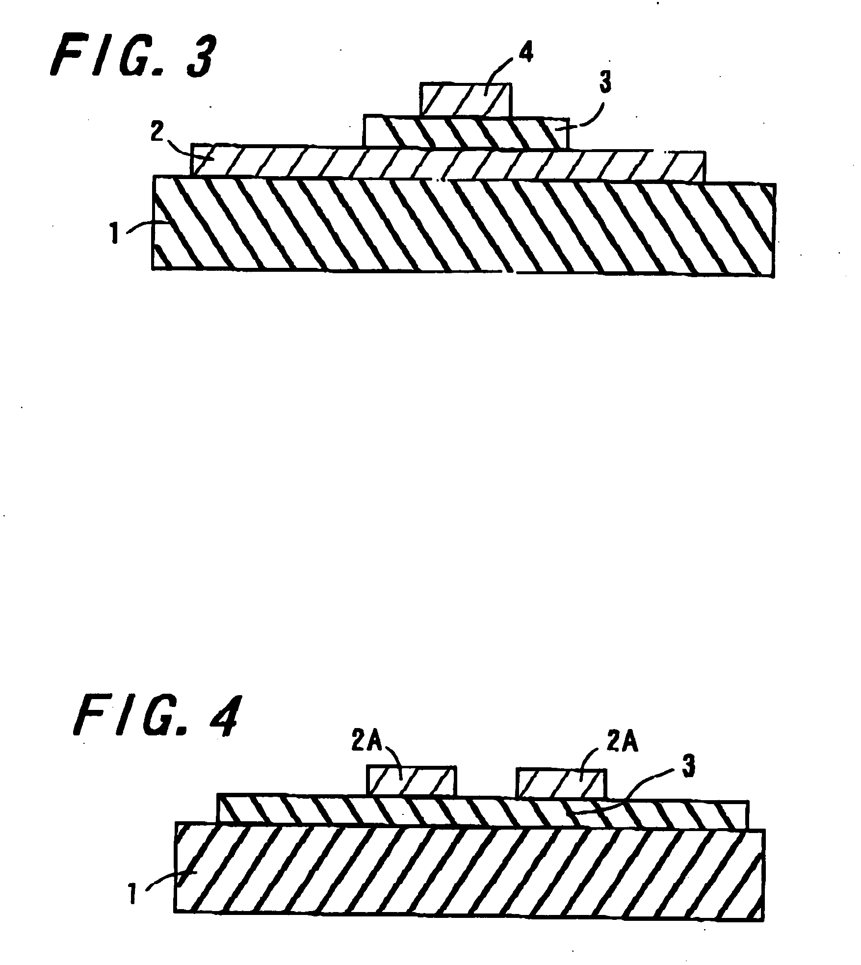
[0062] On a sapphire-made R substrate acting as a supporting substrate were formed a 2 μm-thick lower electrode of Pt; a 0.38 μm-thick dielectric layer of a (Ba0.5Sr0.5) TiO3; and a 0.2 μm-thick upper electrode of Pt successively by means of sputtering, with the temperature of the substrate set at 600° C. Then, using photolithography, the electrodes and the dielectric layer were subjected to patterning by dry etching and wet etching. On the high-dielectric-constant thin film with the upper electrode was formed an insulating layer made of amorphous silicon dioxide by the plasma CVD method. Subsequently, a resist film was coated over the entire surface. Using photolithograp...


PUM


Abstract

A thin film capacitor includes a pair of electrodes and a dielectric layer having piezoelectricity sandwiched therebetween. The phase characteristic of an impedance resulting from application of a voltage to the pair of electrodes peaks periodically according to a frequency of a signal to be inputted or outputted. The frequency of the signal is adjusted to fall in between the values representing the adjacent peaks. Since there are periodic peak values that depend upon the frequency of the inputted or outputted signal, in fabricating a band-pass filter, a higher attenuation can be attained by ensuring that the peak value stands at a low-frequency level. Thus, a higher attenuation can be attained at low frequencies without sacrificing the band-pass characteristic, whereby making it possible to produce a band-pass filter that is excellent in band-pass characteristic.

Description

BACKGROUND OF THE INVENTION [0001] 1. Field of the Invention [0002] The present invention relates to a thin film capacitor constituted with use of a high-dielectric-constant thin film, for example, a variable capacitor for voltage-controlling electrostatic capacitance by exploiting the dependence on an applied voltage of a dielectric constant in a dielectric layer formed of a high-dielectric-constant thin film, and more particularly, to a variable capacitor that operates at high frequencies with a low dielectric loss irrespective of voltage application. The invention relates also to a thin film capacitor constituted with use of a high-dielectric-constant thin film designed for use in power-source decoupling in a semiconductor integrated circuit. [0003] 2. Description of the Related Art [0004] The higher the frequency for use in operations of wireless communication systems, electric circuits, or the like, the greater the demand for electronic components that operate at increasingly h...

Claims


Application Information

Patent Timeline
IPC IPC(8): H01L27/108H01G2/00H01G7/06
CPCH01G7/06
Inventor TAKI, KENJIKISHINO, TETSUYA
Owner KYOCERA CORP
Learn More