

Post-dry etching cleaning liquid composition and process for fabricating semiconductor device
a technology of cleaning liquid composition and semiconductor device, which is applied in the direction of semiconductor/solid-state device details, inorganic non-surface active detergent compositions, instruments, etc., can solve the problems of large environmental burden, insufficient removal performance, and actual etching dimensions that might become larger than intended etching dimensions, etc., to reduce environmental burden and reduce the effect of corrosion
Inactive Publication Date: 2006-01-26
SONY CORP +2
View PDF4 Cites 22 Cited by
- Summary
- Abstract
- Description
- Claims
- Application Information
AI Technical Summary
Benefits of technology
[0018] Under such circumstances, objects of the present invention are to provide a post-dry etching cleaning liquid composition that can remove a residue formed on an etched wall face during dry etching of an insulating film without changing the etching shape and that has a suppressed burden on the environment, and to provide a process for fabricating a semiconductor device, the process being capable of completing dry etching of an insulating film with good shape precision by use of the post-dry etching cleaning liquid composition. It is also an object thereof to improve the adhesion of, for example, a barrier layer to an etched side wall in the damascene process and to thus improve the reliability of the semiconductor device.
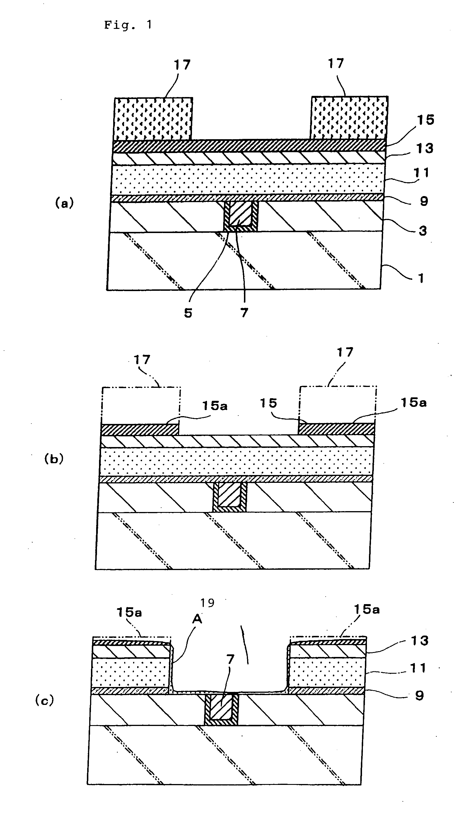
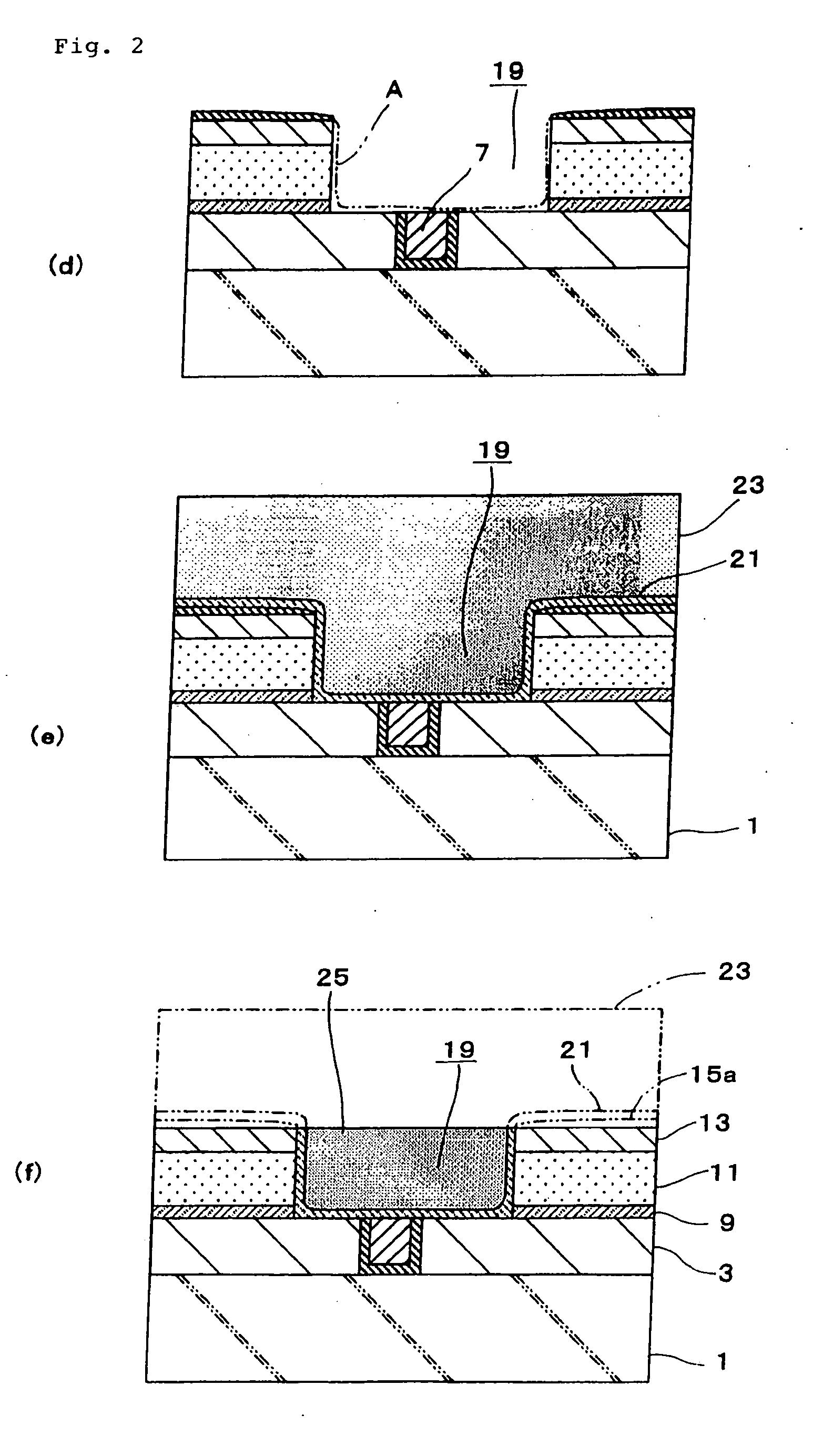
[0024] In such a fabrication process, after the insulating film is patterned by dry etching via the mask pattern, the cleaning posttreatment is carried out using the above-mentioned cleaning liquid composition, and a polymer residue formed as a by-product on an etched wall face during the patterning is thus removed sufficiently by the cleaning liquid composition without corroding a metal material exposed on the etched surface. Moreover, since etching of an altered layer formed on the etched surface during dry etching of the insulating film and etching of the insulating film material forming the treatment surface are suppressed, retreat of an etched side wall can be prevented. EFFECTS OF THE INVENTION
[0026] Furthermore, in accordance with the process for fabricating a semiconductor device of the present invention, by carrying out a cleaning posttreatment, after dry etching of an insulating film, by use of a cleaning liquid composition having the above-mentioned effects, it is possible to remove a residue from the etched surface while maintaining the shape resulting from the etching process, and it is therefore possible to complete the dry etching process with good shape precision. As a result, for example, in the damascene process, it becomes possible to improve the adhesion of a barrier layer to a side wall of a trench pattern formed by dry etching, thereby improving the reliability of the semiconductor device.
Problems solved by technology
That is, with regard to the composition 1), the amount of alkanolamine makes up 40% to 90% of the remover, and the burden on the environment is large.
However, when the composition is used in a single wafer processing system, which has been used frequently in recent years and requires a short processing time, its removal performance is not always sufficient.
Because of this, in posttreatment cleaning for dry etching using this composition, there is a possibility that the actual etching dimensions might become larger than intended etching dimensions.
Because of this, in the above-mentioned damascene process, the adhesion of a barrier layer formed in order to prevent diffusion of a metal wiring material such as copper that is to be embedded in an inner wall of a trench or a via hole formed by etching is insufficient.
There is thus the problem that the metal wiring material diffuses within the insulating film and the resistance of embedded wiring increases.
Method used
View moreImage
Smart ImageViewing Examples

Examples
examples
[0097] Results of evaluation tests described below for cleaning liquid compositions of Examples of the present invention are now explained.
Login to View More PUM
| Property | Measurement | Unit |
|---|---|---|
| Percent by mass | aaaaa | aaaaa |
| Percent by mass | aaaaa | aaaaa |
| Percent by mass | aaaaa | aaaaa |
Abstract
A post-dry etching cleaning liquid composition for cleaning a substrate after dry etching is provided, the cleaning liquid composition containing at least one type of fluorine compound, glyoxylic acid, at least one type of organic acid salt, and water. With regard to the fluorine compound, ammonium fluoride may be used. With regard to the organic acid salt, at least one of ammonium oxalate, ammonium tartarate, ammonium citrate, and ammonium acetate may be used.
Description
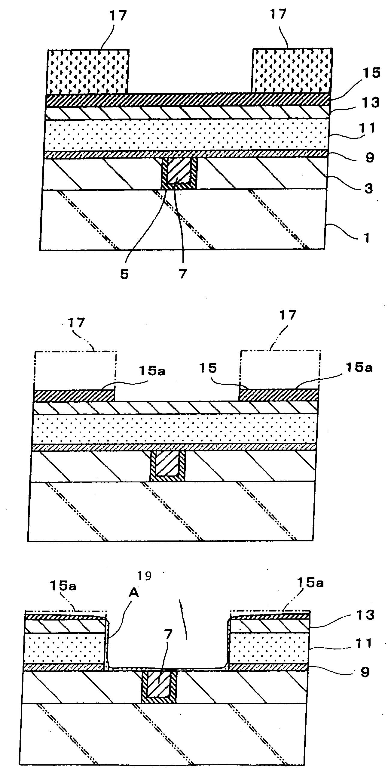
BACKGROUND OF THE INVENTION [0001] 1. Field of the Invention [0002] The present invention relates to a post-dry etching cleaning liquid composition that is used in cleaning for removing a residue after dry etching, and a process for fabricating a semiconductor device using the post-dry etching cleaning liquid composition. [0003] 2. Description of the Related Art [0004] In recent years, accompanying the finer structure of devices due to microfabrication and the increased performance of semiconductor circuit elements, new wiring materials and interlayer insulating film materials have been employed. For example, copper and an alloy having copper as a main component (hereinafter, called a ‘copper alloy’) have been used as new wiring materials for the purpose of reducing wiring resistance and inter-wiring capacitance. Copper wiring is formed by, for example, a damascene process in which, after copper is embedded using sputtering or electro-plating in a trench formed as a wiring pattern i...
Claims
Login to View More Application Information
Patent Timeline
 IPC IPC(8): G03C5/00H01L21/3065C11D3/02C11D3/20C11D3/24C11D7/08C11D7/10C11D7/26C11D7/32C11D11/00C23G1/24H01L21/02H01L21/304H01L21/3205H01L21/336H01L21/768H01L23/52H01L23/522H01L29/78
CPCC11D3/042C11D3/046C11D3/2075C11D3/2082C11D3/2086C11D3/245H01L21/76811C11D7/10C11D7/265C11D7/32C11D11/0047C23G1/24H01L21/02063C11D7/08C11D2111/22H01L21/304
InventorMURAMATSU, MASAFUMIASADA, KAZUMIHAGINO, YUKINOOKUYAMA, ATSUSHINAKAJIMA, TAKAHITOTAKASE, KAZUHIKOUOZUMI, YOSHIHIROMATSUMURA, TSUYOSHIOHWADA, TAKUOISHIKAWA, NORIO
OwnerSONY CORP