
Producing method for crystalline thin film

a technology of crystalline silicon film and production method, which is applied in the direction of crystal growth process, polycrystalline material growth, chemistry apparatus and processes, etc., can solve the problems of insufficient performance of thin film transistors utilizing current melted and resolidified polycrystalline film for the next generation liquid crystal display of widescreen or high-definition, deficient performance of polycrystalline silicon film, and inability to provide such high-performance devices

Inactive Publication Date: 2006-02-02
CANON KK
View PDF17 Cites 24 Cited by
  • Summary
  • Abstract
  • Description
  • Claims
  • Application Information

AI Technical Summary

Benefits of technology

[0027] In the process of melting and resolidification of the film, by taking Tc as a melting point of a bulk crystal and ΔTc as a degree of supercooling causing a spontaneous nucleation from a molten phase, it is also a feature of the present invention to form specific regions with a predetermined interval, at the resolidification of the film, in such a manner that a portion between two specific regions within a predetermined interval assumes a temperature of Tc−ΔTc or higher at a time when the degree of supercooling of an unsolidified region reaches ΔTc. Also the present invention is a method for producing a crystalline film by melting and resolidifying a film with plural heating means. Also the present invention is a method for producing a crystalline film, including a step of giving a constant heat not changing with time, to a film in which regions of mutually different states co-exist in continuation thereby heating to a temperature lower than a melting point, a step of giving a heat changing with time thereby heating and melting the heated film, and a step of resolidifying the film.

Problems solved by technology

However, the thin film transistor utilizing the current melted and resolidified polycrystalline film does not have sufficient performance for the next generation liquid crystal display of widescreen or high-definition.
Also such a polycrystalline silicon film is deficient in performance for use as, for example, a drive circuit element for a plasma display or an electroluminescence display requiring a higher voltage or a larger drive current than in the liquid crystal display, or a high-velocity drive circuit element of a wide screened X-ray image sensor, of which future development is expected.
Even though the defect density within the crystal grains is low, the polycrystalline silicon film with an average grain size in submicron order cannot provide such high-performance devices.
According to the report, the elements showed excellent characteristics in average close to those of elements on a monocrystalline silicon substrate, but a fluctuation among plural elements in the characteristics was far inferior to that of the elements provided on the monocrystalline silicon substrate, falling far short of the expectation.
For example, increased diameter increases the probability of plural crystal grains reaching the hole aperture, so that the selection yield of a single crystal grain becomes low.
Thus it is difficult to retain the crystal grain group 5 in an unmelted state.
Also with the microfabrication technology even up to a near future, it is extremely difficult to form a fine hole of several tens of nanometers or less with a depth of 1 μm.
Furthermore, even when such a fine hole can be actually formed, it is also difficult to fill it with amorphous silicon.
As explained above, the aforementioned technology is an excellent idea cleverly combining the temperature distribution in the direction of depth of the fine hole 2 and the “grain filtering” phenomenon, but it is difficult to increase the selection yield of a single crystal grain for practical use by mere optimization of the conditions in view of the principle and the limitation of the manufacturing technology.

Method used


Image

  • Producing method for crystalline thin film
  • Producing method for crystalline thin film
  • Producing method for crystalline thin film

Examples


example 1-1

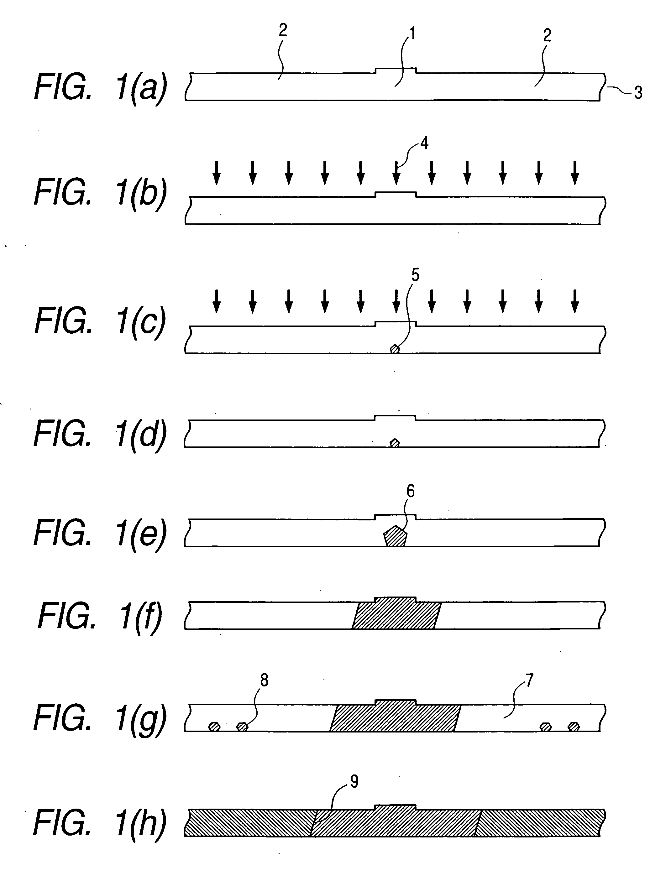
[0169] This Example shows an example of a crystalline silicon film formed by the process of the present invention shown in FIGS. 1(a) to 1(h).

[0170] First, on a substrate (not shown) having an amorphous surface containing silicon oxide etc., an amorphous silicon film 3 of a thickness of 55 nm is formed by vapor phase deposition. Then, by dry etching, the amorphous silicon film is removed by 5 nm from the surface, except for a small region 1 of a diameter of about 1 μm in the plane of the amorphous silicon film. Thus the region 1 of a diameter of about 1 μm has a thickness of 55 nm and the other region 2 has a thickness of 50 nm.

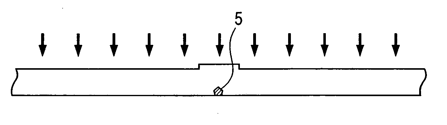
[0171] Then, the starting film is irradiated with a KrF excimer laser light 4 for 30 nsec with an energy density of about 240 mJ / cm2 to melt the starting film, and the film was resolidified to obtain a crystalline film.

[0172] When the crystal grain shape constituting the obtained crystalline film is observed, a single crystal grain of a diameter of about 2...

example 1-2

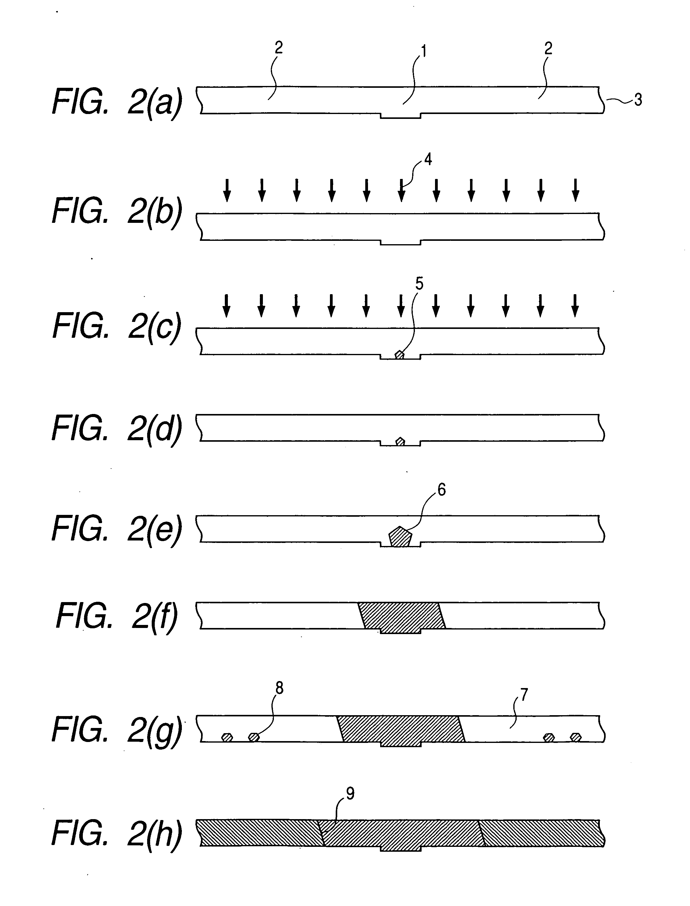
[0177] This Example shows a crystalline silicon film formed by the process shown in FIGS. 2(a) to 2(h).

[0178] First, a substrate (not shown) containing silicon oxide etc. and having an amorphous surface is processed to form on the surface a cylindrical crater of about 0.5 μm in diameter and 10 nm in depth by dry etching. Then, an amorphous silicon film 3 of a thickness of 100 nm is formed on the substrate surface by vapor phase deposition. A cross section of the amorphous silicon film is 105 nm thick at the center of a region 1 of about 0.5 μm in diameter, and 100 nm thick in the region 2 other than the region 1.

[0179] Then, the starting film 3 is irradiated with XeCl excimer laser light 4 for 40 nsec with an energy density of about 310 mJ / cm2 for melting and resolidification, to obtain a crystalline film.

[0180] When the crystal grain shape constituting the obtained crystalline film is observed, a single crystal grain reaching a diameter of 3 μm grown from the small region of the...

example 1-3

[0184] As a third example of the present invention, there is shown a crystalline silicon film formed by steps shown in FIGS. 3(a) to 3(h).

[0185] First, on a substrate (not shown) having an amorphous surface of silicon oxide etc., an amorphous silicon film 3 of a thickness of 55 nm is formed by vapor phase deposition. Then, an etching-resistant masking material (not shown) is provided on the surface of a small region of a diameter of about 1.5 μm in the plane of the amorphous silicon film, and the amorphous silicon film is removed by wet etching by 5 nm from the surface. Thus, in the cross section of the amorphous silicon film 3, a region other than the small region 1 of a diameter of about 1.5 μm has a thickness of 50 nm, while the small region 1 of the diameter of about 1.5 μm has a thickness of 55 nm in a region of a diameter of about 0.7 μm at the center, and the thickness gradually decreases from the external periphery to the outside thus forming a truncated conical shape.

[018...


PUM

PropertyMeasurementUnit
thicknessaaaaaaaaaa
diameteraaaaaaaaaa
diameteraaaaaaaaaa

Abstract

A method for producing a crystalline film by melting and resolidifying a film, characterized in preparing a film having a specific region and obtained either by (A) a step of forming a film in which a “specific region” and an “region continuous to a periphery of the specific region and different in thickness from the specific region” co-exist, or by (B) a step of irradiating a film with an elecrtromagnetic wave or particles having a mass in mutually different conditions between a specific region and a peripheral region thereof, and melting and resolidifying at least a part of the film. As the spatial position of the specific region can be exactly and easily controlled, it is possible to obtain a crystalline film in which a crystal grain is formed in a desired position.

Description

TECHNICAL FIELD [0001] The present invention relates to a crystalline thin film for forming a drive circuit or the like of a flat panel display and a producing method therefor. BACKGROUND ART [0002] In a flat panel display represented by a liquid crystal display, a higher definition, a higher velocity and a larger number of gradation levels in the image display have been achieved by a monolithic formation of a pixel driving circuit on the panel and by improvement in the performance of such a circuit. The panel of simple matrix drive system has progressed to the panel of active matrix drive system employing a switching transistor for each pixel. Also the shift register circuit employed in the active matrix drive system is formed in the peripheral region of the same panel. Thus, there are present full-color, high-definition liquid crystal displays that can even display moving images. [0003] Realization of such a monolithic formation including also a peripheral drive circuit with a pra...

Claims


Application Information

Patent Timeline
Patent Type & Authority Applications(United States)
IPC IPC(8): H01L21/00H01L21/84C30B13/00C30B13/24H01L21/20H01L21/77
CPCC30B13/24C30B29/06H01L21/02422H01L27/1281H01L21/02686H01L21/02689H01L21/02532
Inventor KUMOMI, HIDEYAYAMAZAKI, TAKEOWATANABE, MASATOSHI
Owner CANON KK
Learn More