Substrate inspection apparatus and method

a substrate and apparatus technology, applied in the direction of semiconductor/solid-state device testing/measurement, optical radiation measurement, instruments, etc., can solve the problems of difficult process control in the manufacturing process of wafers, insufficient quality evaluation of all manufactured semiconductors, and limitations in the miniaturization of circuits, etc., to achieve high precision and facilitate operation

Active Publication Date: 2006-02-23
HORIBA LTD
View PDF2 Cites 64 Cited by
  • Summary
  • Abstract
  • Description
  • Claims
  • Application Information

AI Technical Summary

Benefits of technology

[0030] The stress at the microscopic region and the like is measured in high precision using the Raman spectroscopic optical system at the microscopic region of the surface of the sample. That is, the manufacturing process thereof is appropriately adjusted to manufacture a semiconductor substrate forming a thin film applied with stress of an appropriate strength. Further, as the measurement point is observed by including the optical microscope, the operator is able to check the state of the surface of the object through observation, and thus the operation is facilitated.

Problems solved by technology

In order to have the CMOS circuit of high performance and high-speed, a method of shortening the gate length and a method of increasing the carrier speed are proposed, but if the circuit is miniaturized to shorten the gate length, a short channel effect occurs and thus miniaturization of the circuit has limitations.
However, since the stress measurement apparatus disclosed in Japanese Laid-Open Patent Publication No. 8-5471 cannot sequentially and automatically measure the surface of a plurality of wafers, the quality evaluation cannot be sufficiently performed on all the manufactured semiconductor wafers or the semiconductor devices, and an accurate process control in the manufacturing process of the wafer becomes difficult.
Further, in obtaining film thickness in addition to stress for each microfabricated part, it is important to find a correlation between stress and film thickness in manufacturing the semiconductor wafer, but stress and film thickness cannot be measured for the wafer.
In addition, it is supposed that when embedding a thick oxide film such as a trench configuration in the semiconductor device, a particularly significant stress concentration is likely to occur near the microfabricated part.
Thus, if the thick oxide film is formed at the microfabricated part in the sub-100 nm region, stress produced at the interface of the thin films becomes great and heat or stress is generated even when stress similar to when forming a relatively thin oxide film is acted, which may become the cause of defects such as thermal migration or stress migration.
In a laser anneal equipment disclosed in Japanese Laid-Open Patent Publication No. 9-213652, a Raman spectroscopic photometer and an ellipsometer are mounted to allow measurement of structure and index of refraction of the crystalline silicon film immediately after laser anneal, but since the measurement points of the Raman / ellipsometer optical systems differ each other, various physical information at a specific microscopic region cannot be obtained all at once.
Further, an equipment of Japanese Laid-Open Patent Publication No. 9-213652 is included in the equipment of the manufacturing process and thus is difficult to be applied for use as an inspection apparatus.

Method used


Image

  • Substrate inspection apparatus and method
  • Substrate inspection apparatus and method
  • Substrate inspection apparatus and method

Examples


first embodiment

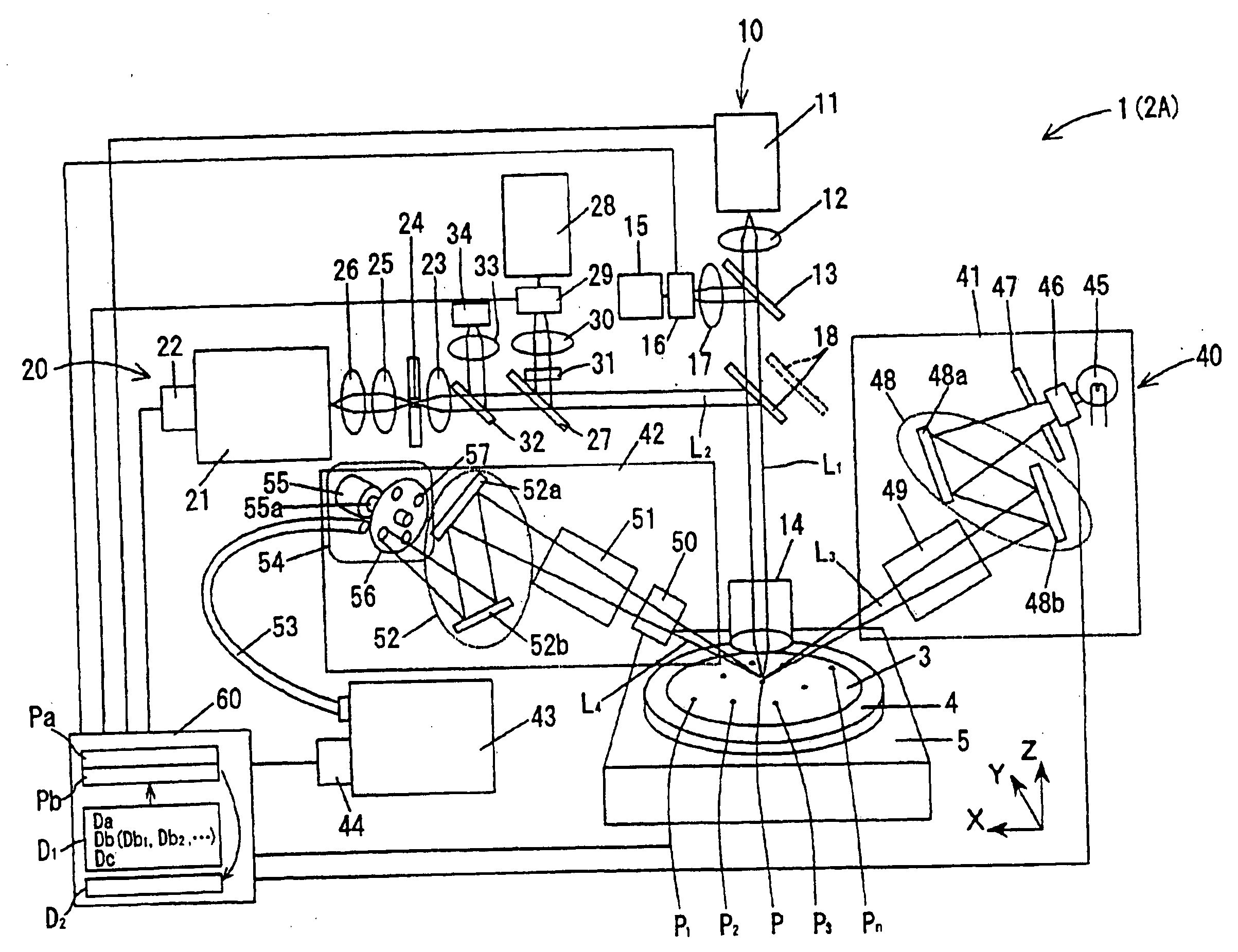
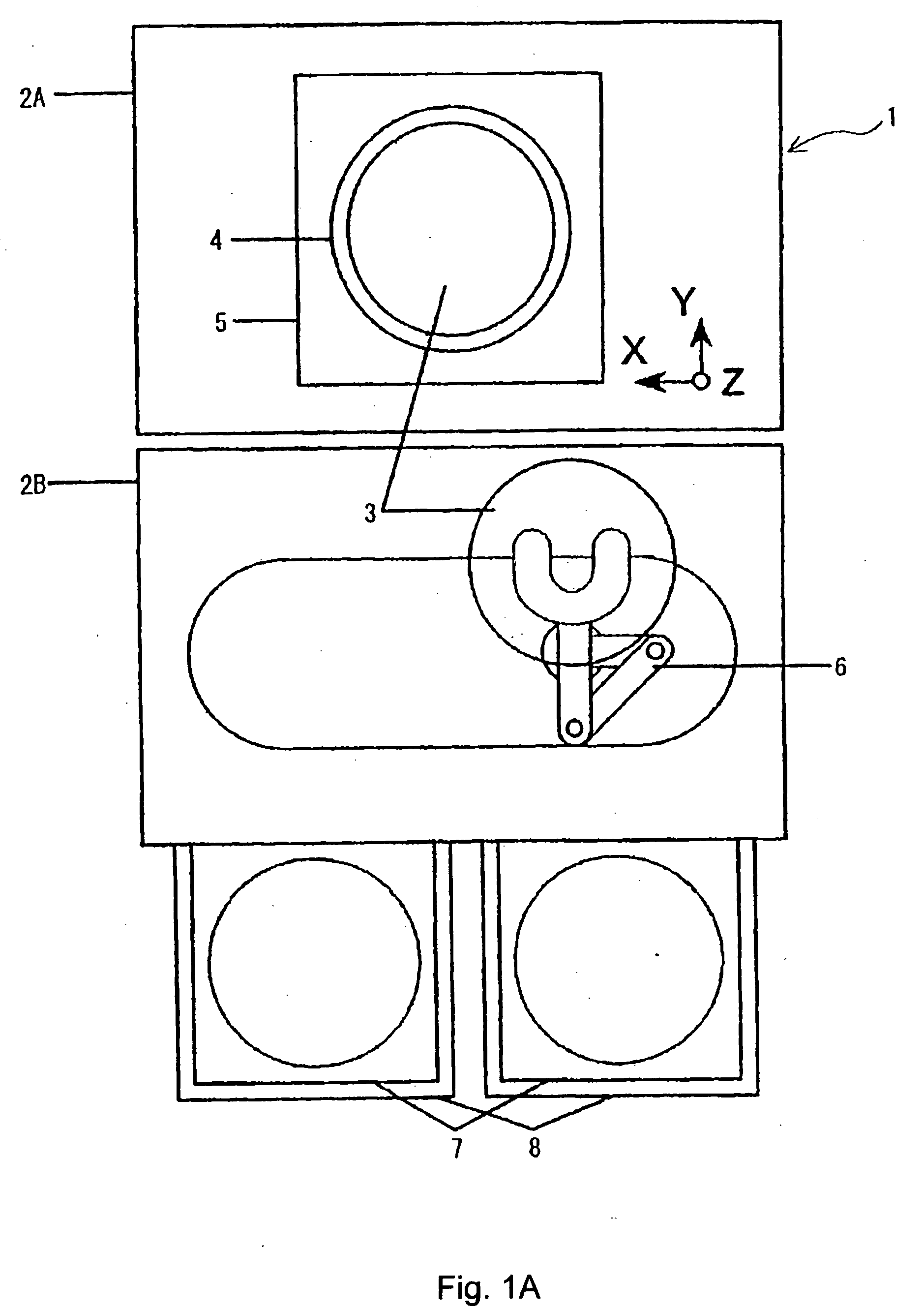
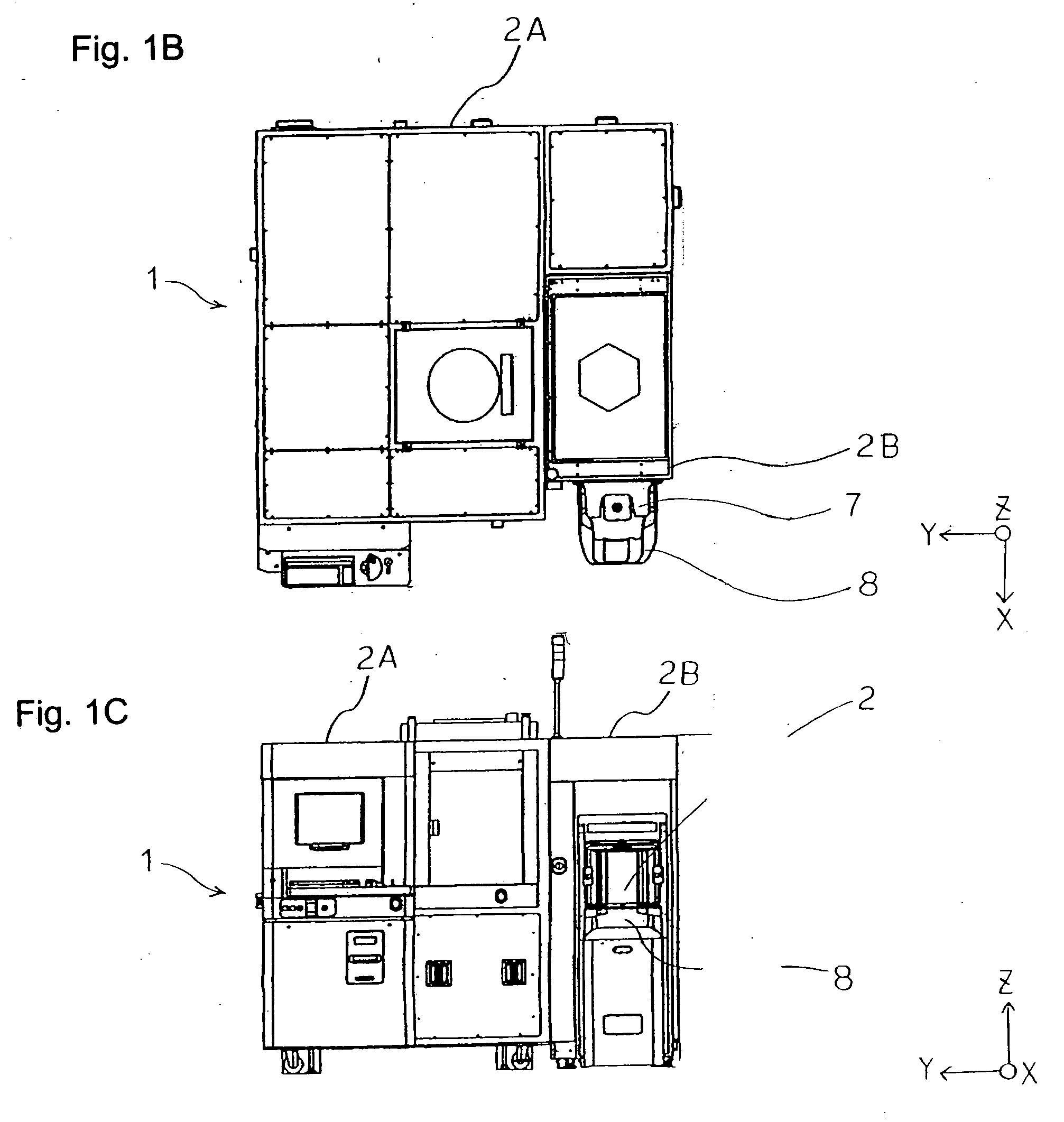
[0048]FIG. 1A is a plan view schematically showing an entire configuration of a substrate inspection apparatus 1 according to the present invention and FIG. 2 is a view showing a configuration of a main part of the substrate inspection apparatus 1. In FIG. 1A, 2A is a measuring chamber of the substrate inspection apparatus 1 equipped with a Raman spectroscopic optical system / ellipsometric optical system, 2B is a transport equipment set up next to the measuring chamber 2A, 3 is a substrate (sample, hereinafter referred to as a wafer) of for example, a silicon wafer formed by applying the strained silicon technique where the thin film of silicon layer is formed on the SiGe layer with large lattice constant, 4 is a sample stage configured so as to be movable in a three-dimensional direction of horizontal direction (X, Y directions) and height direction (Z direction), and 5 is a driving section of the sample stage 4.

[0049] In FIG. 1A, 6 is a robot arm with a function of grasping the waf...

second embodiment

[0113] Further, in the substrate examining device 1A a data calibration sample 72 is arranged at a position in the vicinity of the sample stage 4 close to the wafer 3 to be measured. Desirably, for the data calibration sample 72, those in which the film thickness and the index of refraction are known in advance such as an NIST sample is used for the ellipsometer, and one or a plurality (four in the figure shown) of cut-outs formed by cutting the single crystal silicon without film or the strained silicon in which stress and composition are known in advance into a several dozen mm square is used for the Raman spectroscopy, but the number to be arranged or the type thereof may be selected arbitrarily.

[0114] Other configurations of the substrate examining device 1A according to the second embodiment are the same as those explained in the first embodiment, and thus the same reference characters are denoted for the relevant part or the relevant region, and a detailed explanation thereof...

third embodiment

[0196] According to the substrate examining device 1B of the third embodiment, by selectively and automatically switching and irradiating the laser light of different wavelength from a plurality of laser light sources 28a, 28b, 28c, 28n to the wafer 3 in accordance with the stacked structure of the wafer 3 to be measured and the thickness and the like of the uppermost layer, the distribution in the depth direction (film thickness direction) of stress or composition of the wafer 3 to be measured can be easily and reliably detected without undue influence by the substrate. Thus even having a semiconductor substrate using the strained silicon, as the object to be measured, not only are various physical quantities such as internal stress of the strained silicon and composition of the SiGe layer acting as the base layer reliably measured and the substrate examination is performed at high precision, but further, stress and / or composition of the data calibration sample 72 is measured as ne...


PUM

PropertyMeasurementUnit
wavelengthaaaaaaaaaa
Daaaaaaaaaaa
wavelengthsaaaaaaaaaa

Abstract

The present invention provides a method and substrate examining device that sequentially and automatically measures at least the thickness and the internal stress of the thin film at a predetermined measurement point on the surface of every manufactured semiconductor substrate to perform quality control on each substrate, and reliably recognizes the cause of defects to improve productivity. The examining device and method accurately analyzes the correlation between film thickness and stress to establish the manufacturing processes necessary for manufacturing a semiconductor substrate of higher performance, and measures the distribution of a physical quantity such as internal stress, index of refraction, and composition of the semiconductor substrate in the film thickness direction, without being influenced by change in ambient environmental temperature thereby further improving examination precision.

Description

BACKGROUND OF THE INVENTION [0001] 1. Field of the Invention [0002] The present invention relates to an apparatus and method for inspecting substrates such as semiconductor wafers and liquid crystal panels, more specifically to a substrate inspection apparatus for automatically measuring stress and / or a composition of thin films provided on a surface of a substrate or various patterned microfabricated parts, and further, can provide thickness and the index of refraction of the thin film at the time of measurement. [0003] 2. Description of the Prior Art [0004] In a semiconductor manufacturing process, quality control of a substrate such as a semiconductor wafer is extremely important. Particularly, acquiring physical information such as thickness, index of refraction, stress and composition of the thin film prepared on the surface of the semiconductor wafer and the like and controlling the same so as to be in an appropriate state, is necessary to maintain a stable performance of the ...

Claims


Application Information

Patent Timeline
Patent Type & Authority Applications(United States)
IPC IPC(8): G01N21/00G01N21/95H01L21/66
CPCG01N21/65H01L22/20H01L22/12G01N21/9501
Inventor NAKA, NOBUYUKIKATANISHI, AKIHIROMAGARI, MASAAKINAKAJIMA, YOSHIYUKIARIMOTO, KIMIHIKO
Owner HORIBA LTD
Why Eureka
Try Eureka