Logical operation element field emission emitter and logical operation circuit
a technology of logical operation element and emission emitter, which is applied in the direction of pulse generator, pulse technique, instruments, etc., can solve the problems of limited operating frequency, restricted electron/hole mobility, and degree of integration of vacuum valves capable of high-frequency operation, and achieve high degree of integration and high speed
- Summary
- Abstract
- Description
- Claims
- Application Information
AI Technical Summary
Benefits of technology
Problems solved by technology
Method used
Image
Examples
example 1
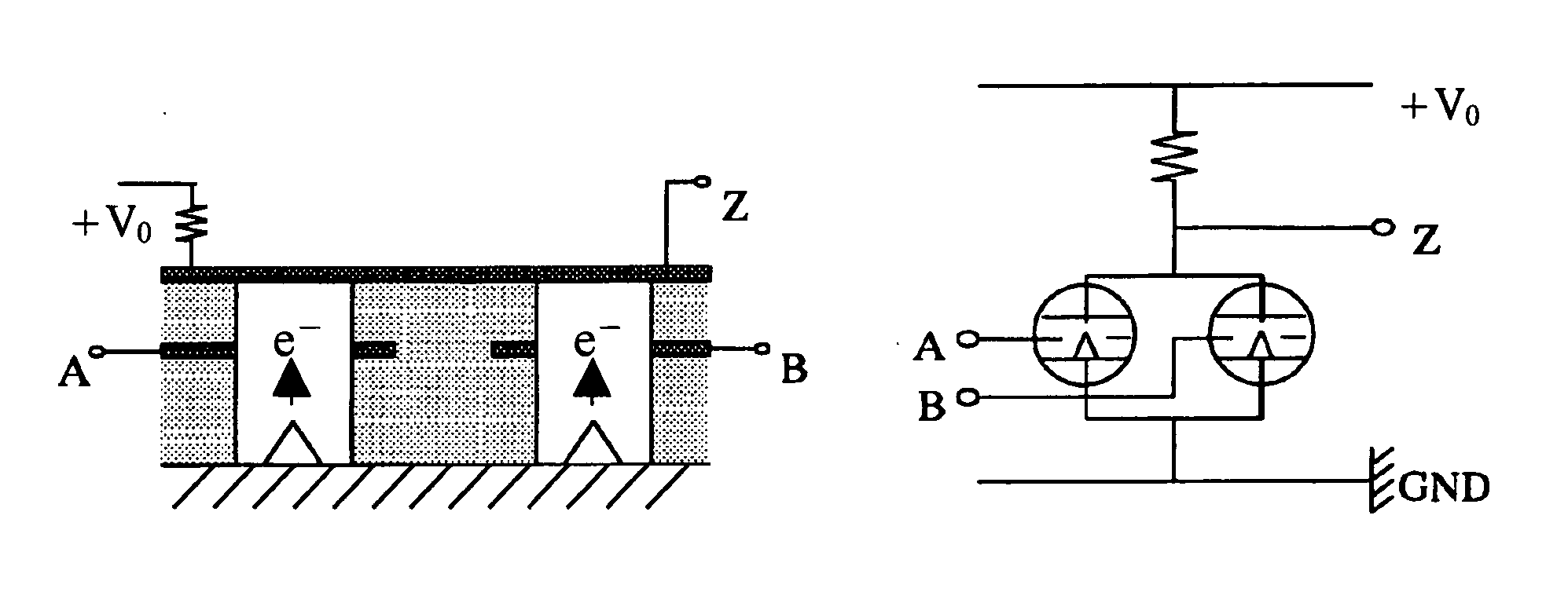
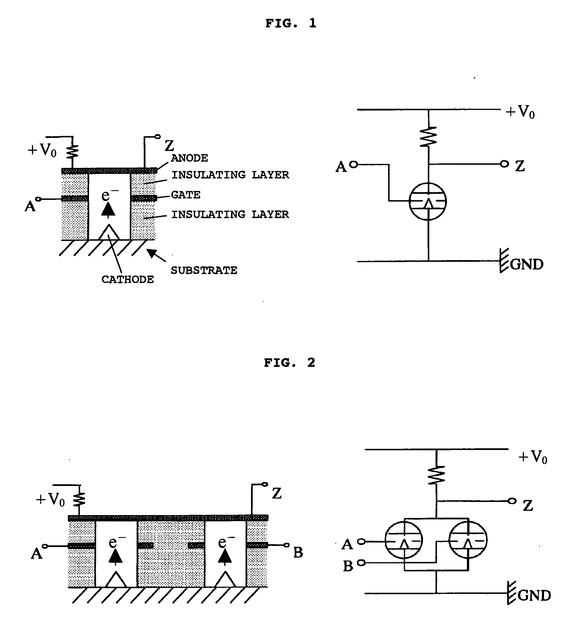
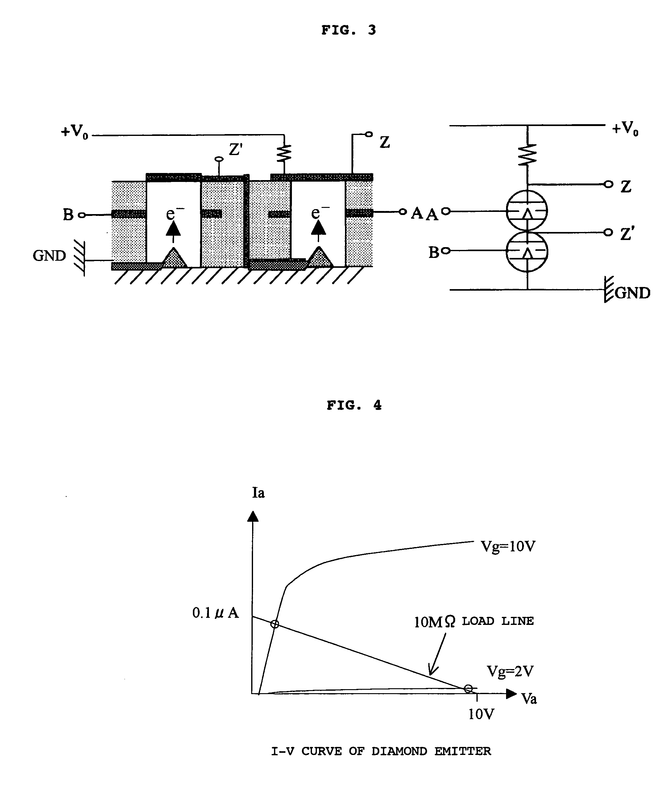
[0071] In this Example, NOT, NOR and NAND elements were manufactured of the basic cross-sectional structure and electrical circuitry shown in FIG. 1 to FIG. 3. The cathodes of the NOT and NOR were grounded and the cathode of the second emitter of the NAND was connected through a pillar-shaped Mo electrode with the anode of the first emitter. The diameter of the pillar-shaped Mo electrode was 0.5 μm. One electron emitter was a Spindt cold cathode, the substrate was SiO2, the cathode was an Mo protrusion, the insulating layer was SiO2, and the gate and anode were Mo. The emitter height was 2 μm, its diameter 0.5 μm, the gate aperture diameter 0.8 μm, the gate height 0.8 μm and the distance between gate and anode was 0.5 μm. In this construction, the gate capacitance Cg was 2.2 pF, and the mutual conductance was 35 ms. The separation between the emitters was 5 μm, and the emitter density was 4×10⁶ emitters / cm2. Elements were manufactured in which emitters of the basic construction of F...
example 2
[0072] In this Example, as the substrate, a diamond substrate comprising an Ib single-crystal synthesized under high pressure, having a (111) plane at the surface was employed. On this diamond substrate, there was formed a phosphorus-doped diamond film of thickness 1 μm, under the conditions: hydrogen 200 sccm, methane 1 sccm, phosphine flow rate PH3 / CH4=0.1%, pressure 100 Torr, sample temperature 870° C., using the method of microwave plasma CVD.
[0073] Next, a film of Al was deposited by the sputtering method and a dot pattern of 1 μmφ was manufactured by a photolithographic process. This was etched to 1.5 μm at a pressure of 50 mTorr, using the conditions: oxygen 50 sccm, CF4 gas 0.5 sccm, by RIB. Projections of height 1 μm were formed, with an electrically conductive P doped region extending from the tip of the projection for 0.5 μm, thereby achieving electrical isolation of the emitters.
[0074]FIG. 4 shows the current voltage characteristic of field electron emission of the emi...
example 3
[0077] As described above, in the case of a NAND element, a relaxation time is required, depending on the input values. Accordingly, the electrode pattern of the NAND element of Example 1 was changed to that shown in FIG. 8 in order to reduce the electrostatic capacitance and decrease the relaxation time. In this pattern, it was arranged that there should be no overlapping area when the anode and the gate of the first emitter were projected onto the element plane. In this way, the electrostatic capacitance was lowered to 1.1 pF and a reduction in the relaxation time was achieved, compared with the prior art design in which there is overlapping.
PUM
 Abstract
Description
Claims
Application Information


