Systems and methods of forming tantalum silicide layers

a technology of silicide layer and metal silicon nitride, which is applied in the direction of coating, chemical vapor deposition coating, capacitor, etc., can solve the problem that the composition of formed metal silicon nitride barrier layer such as ta—si—n cannot be uniform across the substrate surface, and achieve the effect of minimizing detrimental gas phase reactions and improving the control of layer thickness

Inactive Publication Date: 2006-03-09
MICRON TECH INC
View PDF61 Cites 111 Cited by
  • Summary
  • Abstract
  • Description
  • Claims
  • Application Information

AI Technical Summary

Benefits of technology

[0017]“Barrier layer” as used herein refers to a conductive, interfacial layer that can reduce diffusion of ambient oxygen through a dielectric layer into a semiconductor substrate (typically a polysilicon substrate) or can reduce diffusion of one layer into another, such as a copper conductive layer into a semiconductor substrate (typically a polysilicon substrate). For this invention, the barrier layer is a tantalum silicide or tantalum silicon nitride layer.
[0021]“Atomic layer deposition” (ALD) as used herein refers to a vapor deposition process in which numerous consecutive deposition cycles are conducted in a deposition chamber. Typically, during each cycle the metal precursor is chemisorbed to the substrate surface; excess precursor is purged out; a subsequent precursor and / or reaction gas is introduced to react with the chemisorbed layer; and excess reaction gas (if used) and by-products are removed. As compared to the one cycle chemical vapor deposition (CVD) process, the longer duration multi-cycle ALD process allows for improved control of layer thickness by self-limiting layer growth and minimizing detrimental gas phase reactions by separation of the reaction components. The term “atomic layer deposition” as used herein is also meant to include the related terms “atomic layer epitaxy” (ALE) (see U.S. Pat. No. 5,256,244 (Ackerman)), molecular beam epitaxy (MBE), gas source MBE, organometallic MBE, and chemical beam epitaxy when performed with alternating pulses of precursor compound(s), reaction gas and purge (i.e., inert carrier) gas.

Problems solved by technology

However, when PVD methods are used, the stoichiometric composition of the formed metal silicon nitride barrier layers such as Ta—Si—N can be non-uniform across the substrate surface due to different sputter yields of Ta, Si, and N. Due to the resulting poor layer conformality, defects such as pinholes often occur in such layers creating pathways to diffusion.

Method used


Image

  • Systems and methods of forming tantalum silicide layers
  • Systems and methods of forming tantalum silicide layers
  • Systems and methods of forming tantalum silicide layers

Examples


example

Example 1

Pulsed Chemical Vapor Deposition of Tantalum Silicide

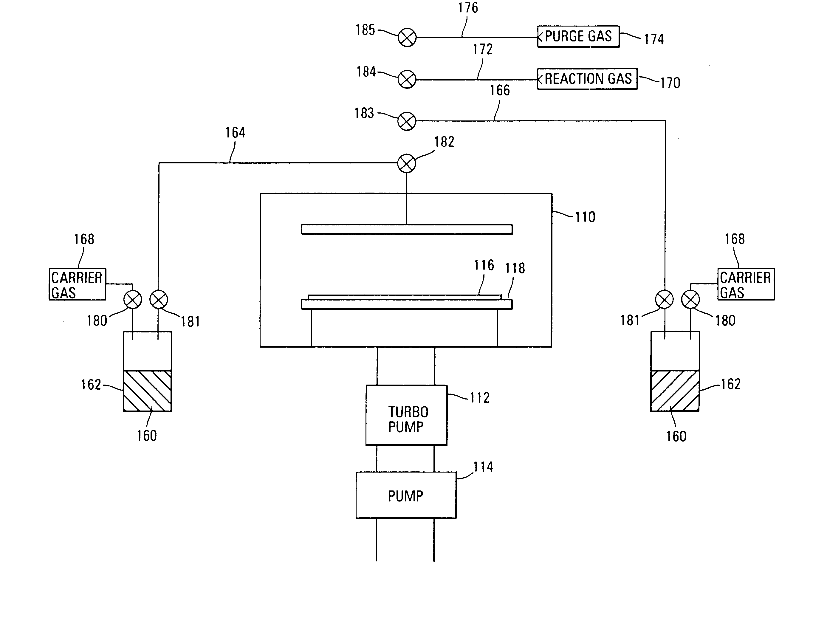
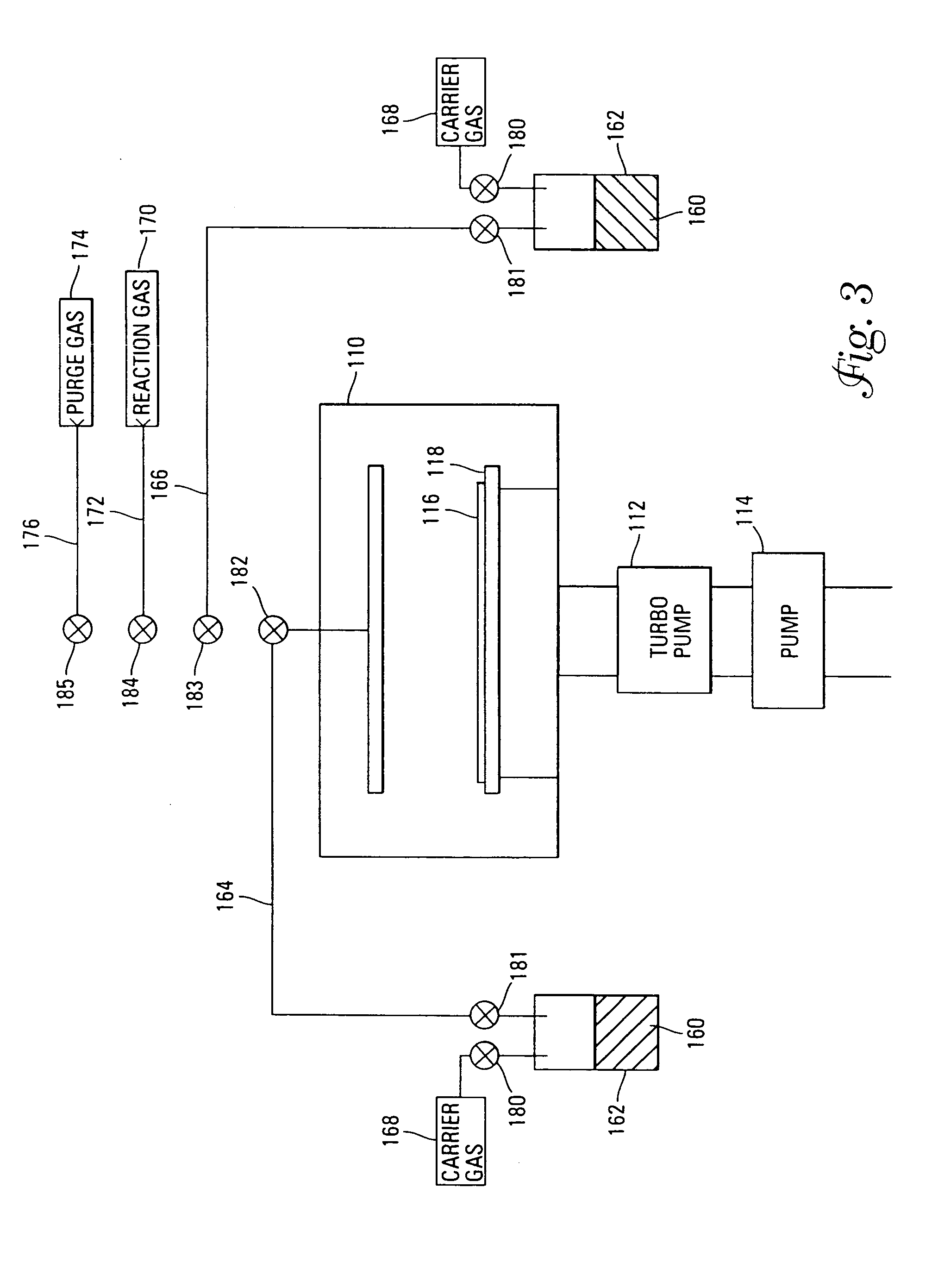
[0064] Using a pulsed CVD method, the following precursor compounds were pulsed for 200 cycles in a deposition chamber as described in FIG. 3 containing a borophosphosilicate glass (BPSG) substrate, each cycle consisting of pulses in the following order: (1) tantalum pentafluoride (Alfa Aesar, Ward Hill, Mass.; and (2) disilane (VOC Gases). During each cycle, excess amounts of each precursor compound not chemisorbed were purged from the chamber after chemisorption and prior to the introduction of the next precursor compound using an argon sweep at 30 mL / min and a vacuum pump. The substrate temperature was kept at approximately 275° C. throughout the entire deposition process.

[0065] At the end of the process, a 1700 Å thick miffor-like layer of tantalum silicide was formed having a resistivity of 255 μΩ-cm. The layer contained tantalum, silicon, and a trace of oxygen as determined by x-ray photoelectron spectroscopy (XP...


PUM

PropertyMeasurementUnit
temperatureaaaaaaaaaa
pressureaaaaaaaaaa
adsorption energiesaaaaaaaaaa

Abstract

A method of forming (and apparatus for forming) tantalum silicide layers (including tantalum silicon nitride layers), which are typically useful as diffusion barrier layers, on a substrate by using a vapor deposition process with a tantalum halide precursor compound, a silicon precursor compound, and an optional nitrogen precursor compound.

Description

[0001] This is a divisional of U.S. patent application Ser. No. 10 / 229,813, filed Aug. 28, 2002, (pending), which is incorporated herein by reference.FIELD OF THE INVENTION [0002] This invention relates to methods of forming tantalum layers containing silicon (suicide layers) and optionally nitrogen (silicon-nitride layers) on substrates using a vapor deposition process. The formed tantalum-containing layers are particularly useful as diffusion barriers for polysilicon substrates to reduce diffusion of oxygen, copper, or silicon. BACKGROUND OF THE INVENTION [0003] In very-large-scale integration (VLSI) technology, tantalum suicide has been proposed to be useful in a variety of applications. These include: policide gate metallization (i.e., the use of tantalum silicide in combination with a doped polycrystalline silicon (poly-Si) underlayer as a low resistive gate metallization layer); silicide gate (i.e., the use of tantalum silicide as a directly deposited layer on a gate oxide to ...

Claims


Application Information

Patent Timeline
Patent Type & Authority Applications(United States)
IPC IPC(8): C23C16/00C23C16/08C23C16/30C23C16/44C23C16/455H01L21/285H01L21/768
CPCC23C16/08C23C16/30C23C16/42C23C16/45523H01L28/57H01L21/28556H01L21/28562H01L21/76843H01L21/7687C23C16/45553
Inventor VAARTSTRA, BRIAN A.
Owner MICRON TECH INC
Why Eureka
Try Eureka