Top layers of metal for integrated circuits

a technology of integrated circuits and top layers, which is applied in the direction of semiconductor devices, semiconductor/solid-state device details, inductances, etc., can solve the problems of increasing the negative impact of circuit performance, significantly reducing the performance of chips, and affecting the performance of high-performance integrated circuits. achieve the effect of improving the performance of high-performance integrated circuits

Active Publication Date: 2006-03-23
QUALCOMM INC
View PDF69 Cites 106 Cited by
  • Summary
  • Abstract
  • Description
  • Claims
  • Application Information

AI Technical Summary

Benefits of technology

[0013] It is the primary objective of the present invention ...

Problems solved by technology

The metal connections which connect the Integrated Circuit to other circuit or system components become of relative more importance and have, with the further miniaturization of the IC, an increasingly negative impact on the circuit performance.
The capacitance and resistance of the metal interconnections increase, which degrades the chip performance significantly.
Attempts to reduce the resistance by using wider metal lines result in higher capacitance of these wires.
It is technically difficult and economically expensive to create thicker t...

Method used


Image

  • Top layers of metal for integrated circuits
  • Top layers of metal for integrated circuits
  • Top layers of metal for integrated circuits

Examples


Embodiment Construction

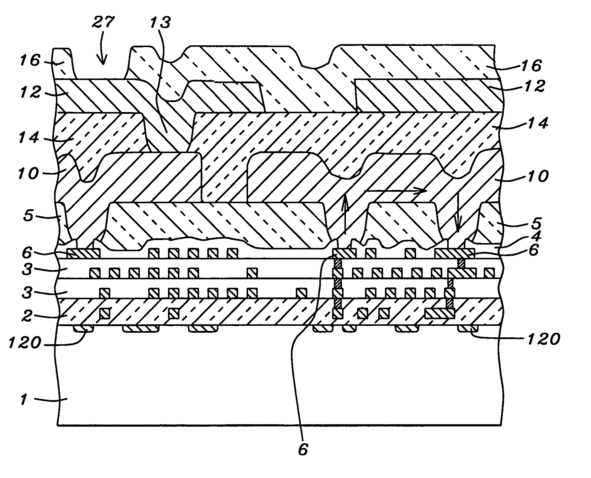
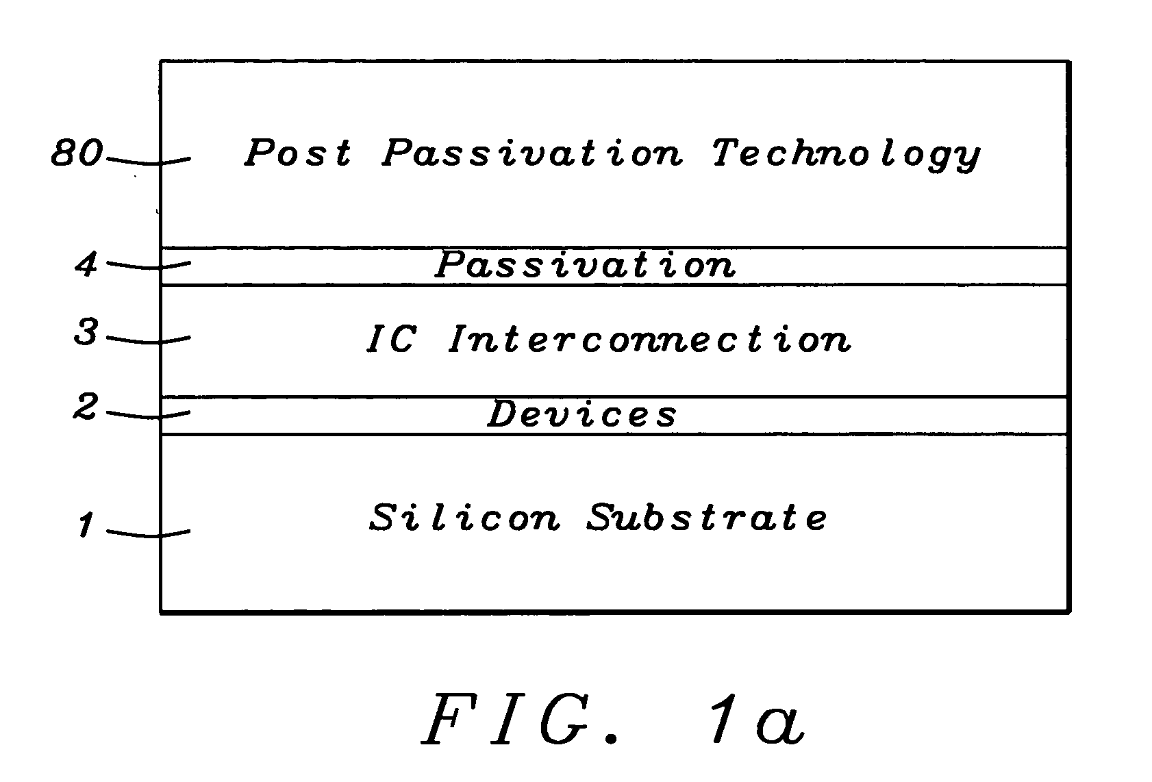
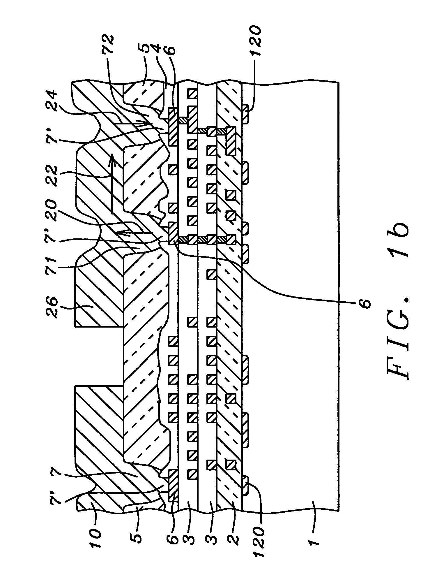
[0043] The present invention teaches an Integrated Circuit structure where key re-distribution and interconnection metal layers and dielectric layers are added over a conventional IC. These re-distribution and interconnection layers allow for wider buses and reduce conventional RC delay.

[0044]FIG. 1a shows a cross-sectional representation of a general view of the invention. Devices 2 are formed in and on a semiconductor substrate 1. These may be n-channel MOS devices, p-channel MOS devices, and / or CMOS devices. Metallization is accomplished in one or more layers of IC Interconnection 3, above the device layer. These metal layers are referred to as fine line metal interconnections. Typically, the intermetal dielectric (IMD) layers comprise silicon-based oxides, such as chemical vapor deposited (CVD) silicon oxide, CVD TEOS oxide, spin-on-glass (SOG), fluorosilicate glass (FSG), high density plasma CVD oxides, or the composite layer formed by a portion of this group of materials. The...


PUM


Abstract

The present invention adds one or more thick layers of polymer dielectric and one or more layers of thick, wide metal lines on top of a finished semiconductor wafer, post-passivation. The thick, wide metal lines may be used for long signal paths and can also be used for power buses or power planes, clock distribution networks, critical signal, and re-distribution of I/O pads.

Description

RELATED PATENT APPLICATIONS [0001] This is a continuation-in-part application of MEG-04-014, Ser. No. 10 / 948020, filed on Sep. 23, 2004, which is related to attorney docket number MSL98-002CCCCIP Ser. No. 10 / 154,662 filed on May 24, 2002, a continuation-in-part application of Ser. No. 10 / 058,259, filed on Jan. 29, 2002, now issued as U.S. Pat. No. 6,660,728, which is a continuation application of Ser. No. 09 / 251,183, filed on Feb. 17, 1999, now issued as U.S. Pat. No. 6,383,916, which is a continuation-in-part application of Ser. No. 09 / 216,791, filed on Dec. 21, 1998, abandoned, all of which are herein incorporated by reference in their entirety.BACKGROUND OF THE INVENTION [0002] (1) Field of the Invention [0003] The invention relates to the manufacturing of high performance, high current, low power, and / or low voltage Integrated Circuit (IC's), and more specifically to methods of achieving high performance of the Integrated Circuits by reducing the capacitance and resistance of in...

Claims


Application Information

Patent Timeline
IPC IPC(8): H01L21/4763
CPCH01L21/768H01L21/76804H01L21/76838H01L21/7685H01L21/76885H01L23/522H01L23/5222H01L23/5223H01L23/5227H01L23/5228H01L23/525H01L23/5283H01L23/5286H01L23/53238H01L23/5329H01L23/60H01L24/02H01L24/10H01L24/11H01L27/0676H01L27/08H01L28/10H01L28/20H01L2224/0231H01L2224/0401H01L2224/04042H01L2224/04073H01L2224/05568H01L2224/05644H01L2224/13099H01L2924/01013H01L2924/01015H01L2924/01022H01L2924/01027H01L2924/01029H01L2924/01046H01L2924/01047H01L2924/01073H01L2924/01074H01L2924/01075H01L2924/01078H01L2924/01079H01L2924/01082H01L2924/04941H01L2924/04953H01L2924/12044H01L2924/14H01L2924/15174H01L2924/15184H01L2924/15192H01L2924/15311H01L2924/30105H01L2224/0558H01L2924/01006H01L2924/01019H01L2924/01024H01L2924/01033H01L2924/014H01L2224/16225H01L2924/0002H01L24/13H01L2924/00H01L2224/05552H01L2224/13H01L2924/0001H01L24/05H01L24/16H01L2224/05548H01L2224/02311H01L2224/02
Inventor LIN, MOU-SHIUNGCHOU, CHIU-MINGCHOU, CHIEN-KANG
Owner QUALCOMM INC
Why Eureka
Try Eureka