Semiconductor integrated circuit device and method of manufacturing the same

Active Publication Date: 2006-06-01
RENESAS ELECTRONICS CORP
View PDF9 Cites 217 Cited by
  • Summary
  • Abstract
  • Description
  • Claims
  • Application Information

AI Technical Summary

Benefits of technology

[0029] The thermal retention characteristic of the phase change memory is improved by the increase in the phase change temperature and the memory retention guaranteed (10 years' information retention) operation temperature for the memory can be improved to greatly extend the kinds of t

Problems solved by technology

In a case where the temperatures capable of guaranteeing long time storage of memory are such low temperatures as described above, the range for utilizing the semiconductor integrated circuit device mounting the phase change memory is extremely limited.
Such a current gives a significant trouble in obtaining a phase change memory of large capacity.
However, as a result of applying such a material to a pha

Method used


Image

  • Semiconductor integrated circuit device and method of manufacturing the same
  • Semiconductor integrated circuit device and method of manufacturing the same
  • Semiconductor integrated circuit device and method of manufacturing the same

Examples


example 1

[0127] In the example, the progress of the experiment for solving the problem relating to the invention and the phenomena found therein are mainly explained. For the preparation of a chalcogenide film as a main portion of the invention, a sputtering apparatus was used. The outline is shown in FIG. 14. A usual apparatus may suffice as the sputtering apparatus. For example, a sample holding substrate 52, and a heater 55 and a target 51 which are opposed to the sample holding substrate 52 are placed in a vacuum chamber 50. An evacuation end 54 is disposed at one end of the vacuum chamber 50. The temperature is made variable from about −33° C. to 300° C. Various gas introduction ends 53 are disposed at the other end of the vacuum chamber 50. Gases are for example Ar, nitrogen oxygen, CH3, CO2, etc. in this example.

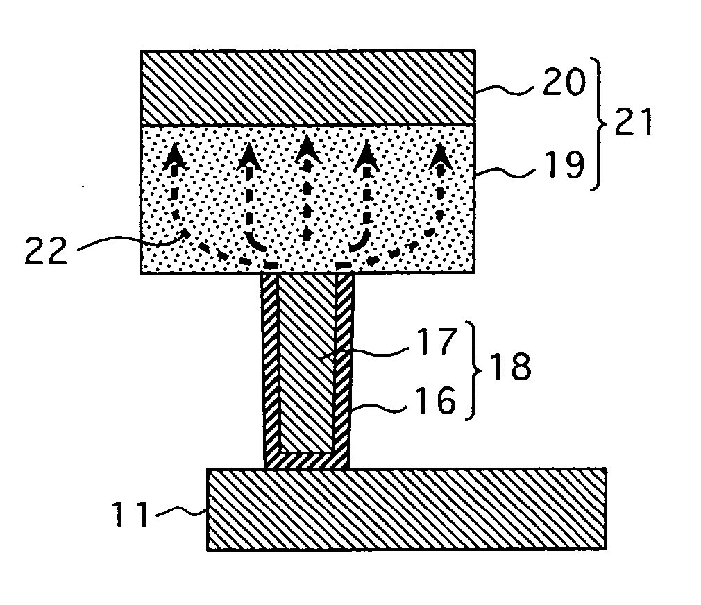
[0128] On the tungsten plug 18 described previously, the GST film 19 was formed by using the sputtering apparatus for preparing the phase change memory device 21 comprising t...

example 2

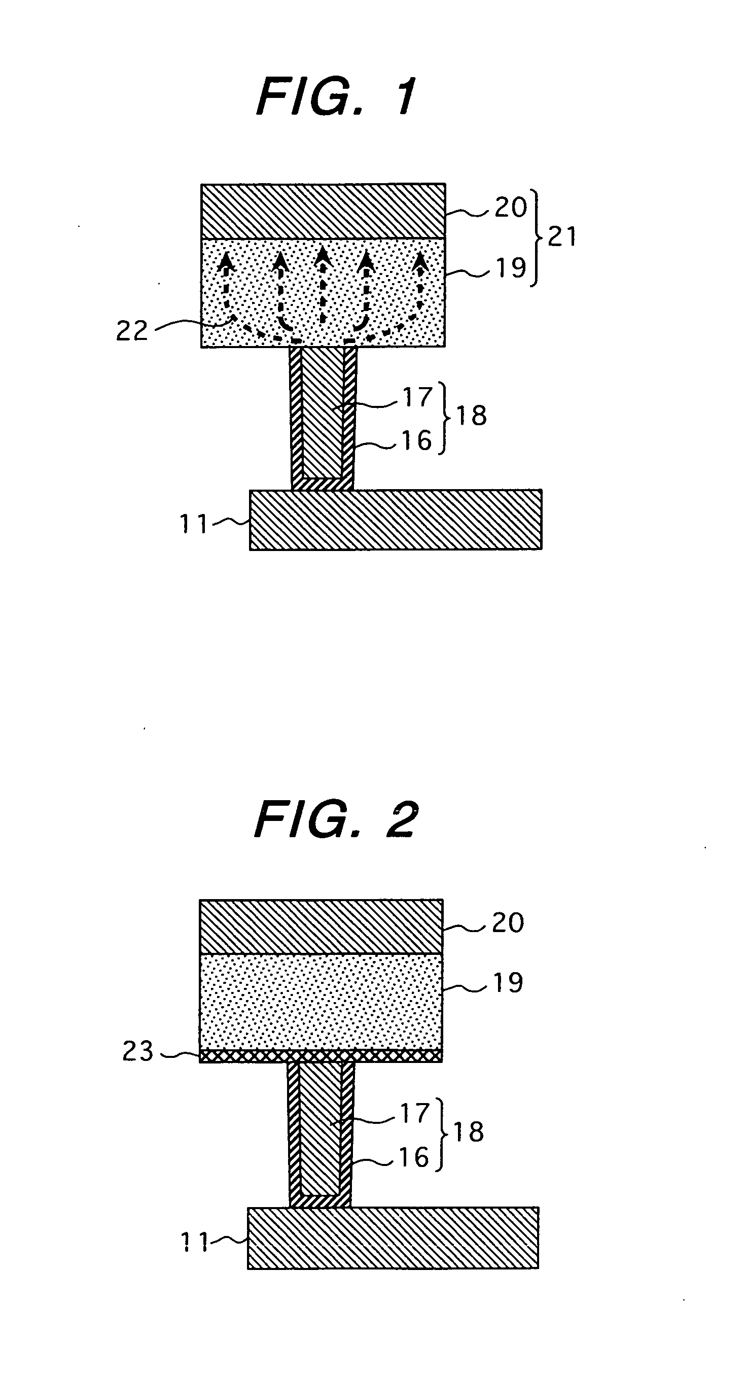
[0143] In the phase change memory of Example 1, a predetermined amount of germanium nitride is formed over the entire chalcogenide film. Example 2 uses a composite GST film.

[0144] In this example, as shown in FIG. 6, a first GST film 27 of 20 nm thickness was formed at first at a mixing ratio of 2% nitrogen gas and argon gas and, successively, a second GST film 28 of 80 nm thickness was formed by using only the argon gas to form a composite GST film as a memory film of a phase change memory. In this structure, nitrogen diffused from the first GST film to the second GST film in the thermal step at 450° C. after formation of the composite film to form a concentration gradient of a germanium nitride compound from the vicinity of the plug boundary to the second GST film. Near the boundary, about 50% of the existent germanium formed a nitride compound and the remaining portion contributed to GST crystals, which was decreased to several % near the surface of the second GST film. In this ...

example 3

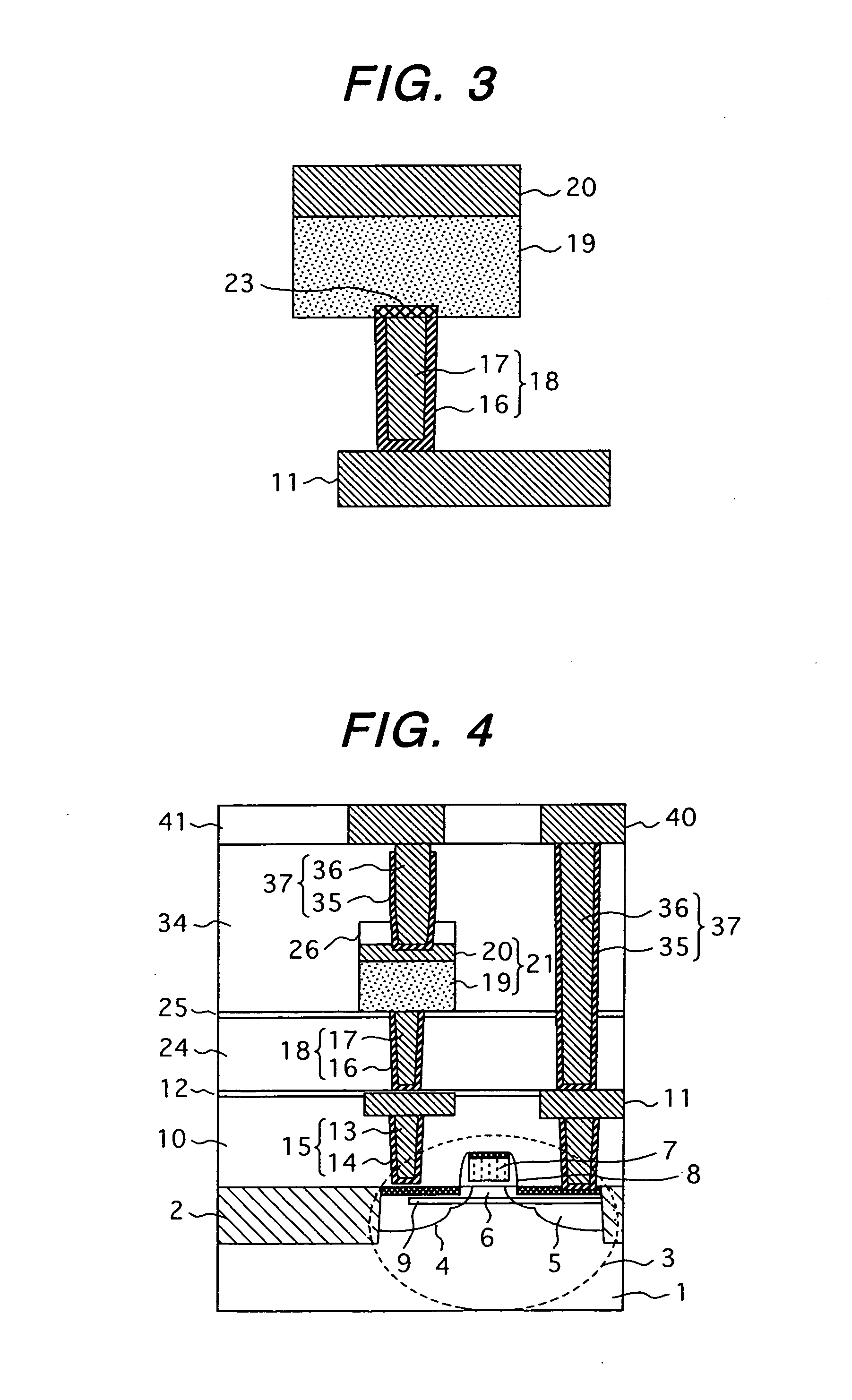
[0148] In Example 2, the GST film was formed by two stages divisionally so as to increase the concentration of germanium nitride in the GST film near the plug boundary. Example 3 shows an example of forming tungsten nitride on the surface of the tungsten plug.

[0149] In this example, the surface of the tungsten was previously nitrided by nitrogen plasma to form a tungsten nitride of about 10 nm thickness. Then, a GST film of 100 nm thickness was formed at an addition nitrogen gas mixed flow rate ratio of 0.01%. In this example, the GST film comprised a single layer. The tungsten nitride is extremely instable and easily releases nitrogen. Accordingly, in the phase change memory device formed by using such a structure, nitrogen released from the tungsten nitride and germanium of the GST film were mainly reacted in the thermal step necessary for the manufacture of the semiconductor integrated circuit device, to form a germanium nitride only near the plug boundary in a self-alignment ma...


PUM


Abstract

Disclosed herein is a phase change memory semiconductor integrated circuit device using a chalcogenide film that solves a problem that the operation temperature capable of ensuring long time memory retention is low due to low phase change temperature is and, at the same time, a problem that power consumption of the device is high since a large current requires to rewrite memory information due to low resistance. A portion of constituent elements for a chalcogenide comprises nitride, oxide or carbide which are formed to the boundary between the chalcogenide film and a metal plug as an underlying electrode and to the grain boundary of chalcogenide crystals thereby increasing the phase change temperature and high Joule heat can be generated even by a small current by increasing the resistance of the film.

Description

CLAIM OF PRIORITY [0001] The present application claims priority from Japanese application JP 2004-348647, filed on Dec. 1, 2004, the content of which is hereby incorporated by reference into this application. BACKGROUND OF THE INVENTION [0002] The present invention relates generally to a semiconductor integrated circuit device and a manufacturing technique thereof and, more specifically, it relates to a semiconductor integrated circuit device including a structural portion formed by stacking a chalcogenide film on a conductive plug, as well as a technique which is effectively applied to the manufacture thereof. [0003] Semiconductor memories include a volatile DRAM (Dynamic Random Access Memory) and a non-volatile memory semiconductor integrated circuit device such as a flash memory. An increase in the integration degree for each of the memories requires miniaturization of a memory device (cell) and the technology node (technical generation of design dimension) is going to reach the...

Claims


Application Information

Patent Timeline
IPC IPC(8): H01L29/04
CPCH01L45/06H01L45/1233H01L45/126H01L45/144H01L45/1625H01L45/1641H01L45/165H01L27/2436H01L45/122H10B63/30H10N70/821H10N70/8413H10N70/231H10N70/026H10N70/826H10N70/041H10N70/043H10N70/8828H10B12/00
Inventor YAMAMOTO, NAOKITAKAURA, NORIKATSUMATSUI, YUICHIMATSUZAKI, NOZOMUKUROTSUCHI, KENZOTERAO, MOTOYASU
Owner RENESAS ELECTRONICS CORP
Why Eureka
Try Eureka