Method for fabricating a first contact hole plane in a memory module

a memory module and first contact technology, applied in the direction of basic electric elements, electrical equipment, semiconductor devices, etc., can solve the problems of the protective layer of the gate electrode track being concomitantly attacked, and the short circuit between the bit line contact and the gate electrode track. , to achieve the effect of simple and reliabl

Inactive Publication Date: 2006-07-06
INFINEON TECH AG
View PDF13 Cites 28 Cited by
  • Summary
  • Abstract
  • Description
  • Claims
  • Application Information

AI Technical Summary

Benefits of technology

[0011] It is an object of the invention to provide an optimized process implementation for fabricating a first contact hole plane of a memory module, which is dist

Problems solved by technology

In this case, however, the formation of the contact holes in the logic region for the purpose of fabricating the substrate and gate electrode track contacts is effected separately from the formation of the contact holes for the bit line contacts in the cell array region by an autonomous lithography process, since there is otherwise the risk of damaging the gate electrode tracks around the bit line contacts during the contact hole etching, which may then lead to a short circuit between the bit line contacts and the gate electrode tracks.
If the contact holes for the bit line contacts are also opened at the same time during this etching, there is the risk of the protective layer of the gate electrode tracks being concomitantly attacked and damaged around the bit line contacts, which may then lead to a s

Method used


Image

  • Method for fabricating a first contact hole plane in a memory module
  • Method for fabricating a first contact hole plane in a memory module
  • Method for fabricating a first contact hole plane in a memory module

Examples


Embodiment Construction

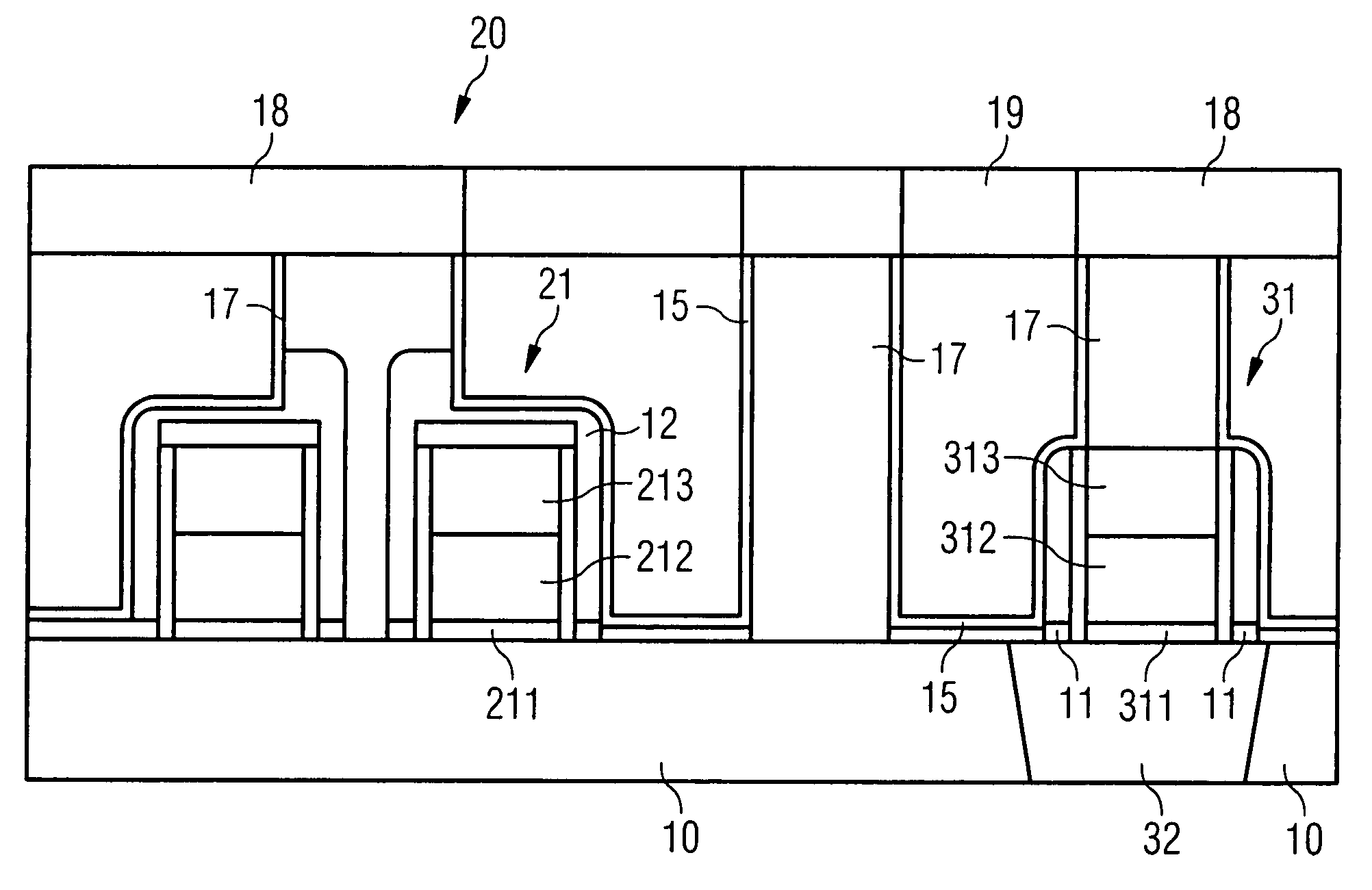
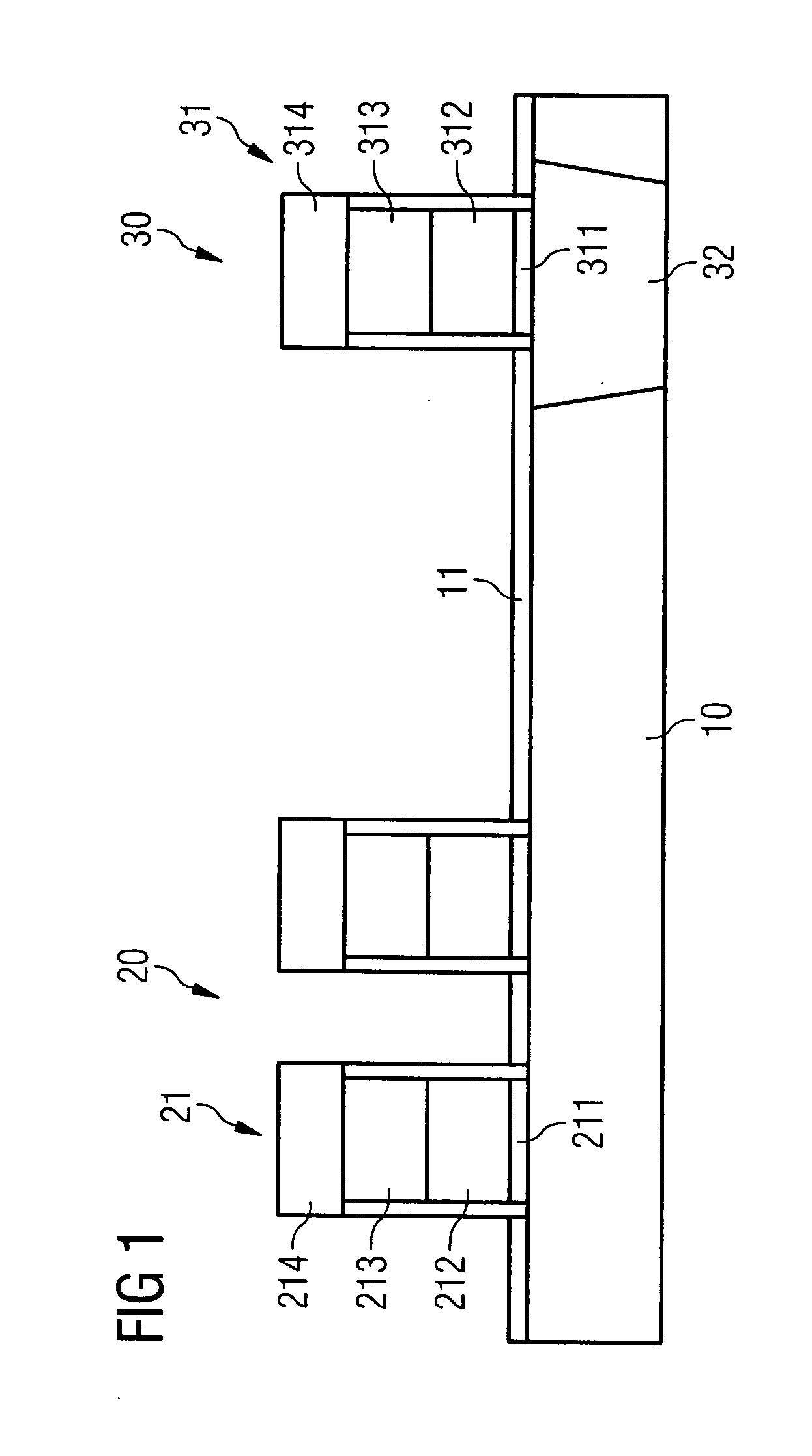
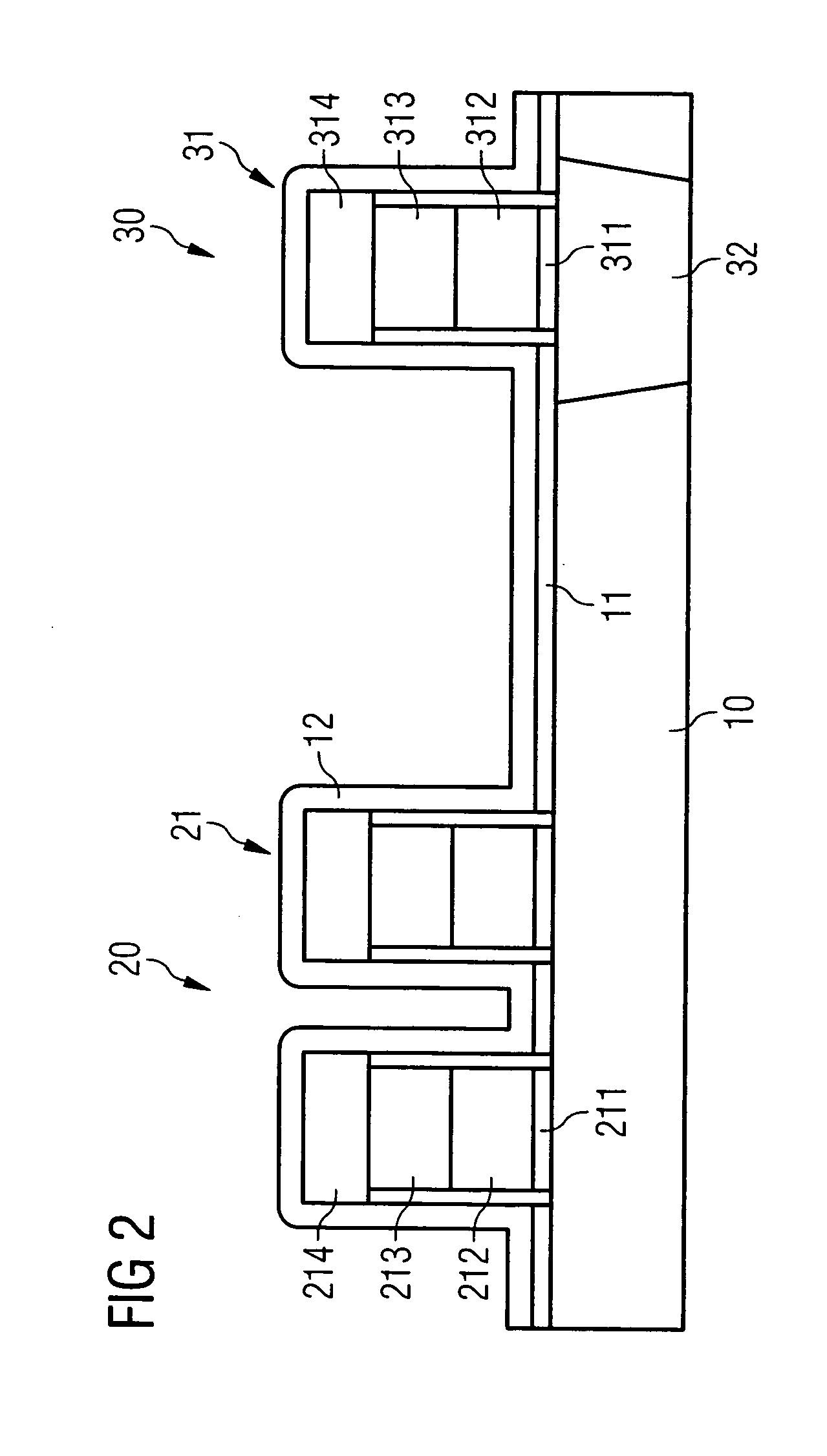
[0028] The invention is explained by way of example on the basis of a process sequence for fabricating a first contact hole plane in a DRAM module with a cell array region and a logic region on a silicon wafer. However, it can also be used for other memory modules, e.g. embedded DRAM or SRAM modules, in which contacts are to be embodied simultaneously in a cell array region and a logic region.

[0029] The figures in each case illustrate a cross section through a detail from a pre-patterned silicon wafer on which a cell array region and a peripheral logic region are provided. In this case, the memory cells of the DRAM are composed of a selection transistor (not shown) and a storage capacitor (not shown). The peripheral logic region contains various elements, in particular switching transistors (not shown) for addressing the memory cells. Trench isolations, so-called STI regions (shallow trench isolation), are formed for the purpose of insulating the different components in the cell ar...


PUM


Abstract

A silicon dioxide layer is formed and a mask layer is deposited and then patterned to produce openings in the mask layer in the region around the gate contacts onto the gate electrode tracks in the logic region. The surface is uncovered around the gate contacts to the gate electrode tracks in the logic region, reducing the silicon dioxide layer. A sacrificial layer covering the gate electrode tracks is formed and patterned to form sacrificial layer blocks above the contact openings for the bit line contacts between the mutually adjacent gate electrode tracks in the cell array region and above the contact openings for the substrate contacts to the semiconductor surface and the gate contacts onto the gate electrode tracks in the logic region. A filling layer is formed between the sacrificial layer blocks, and the sacrificial layer blocks are removed. The contact opening regions are filled with conductive material.

Description

CLAIM FOR PRIORITY [0001] This application claims priority to German Application No. 10 2004 020 938.3-33, filed Apr. 28, 2004, which is incorporated herein, in its entirety, by reference. TECHNICAL FIELD OF THE INVENTION [0002] The invention relates to a method for fabricating a first contact hole plane of a memory module. More specifically, the invention relates to fabricating a first contact hole plane of a dynamic random access memory (DRAM). BACKGROUND OF THE INVENTION [0003] DRAMs are composed of a multiplicity of memory cells which are formed regularly in the form of a matrix on a semiconductor wafer. The memory cells in this case have a storage capacitor and a selection transistor, the selection transistor generally being a field effect transistor. During a write or read operation, the storage capacitor is charged or discharged, via the selection transistor, with an electrical charge corresponding to the respective data unit (bit). For this purpose, the selection transistor ...

Claims


Application Information

Patent Timeline
IPC IPC(8): H01L21/4763H01L21/283H01L21/60H01L21/768H01L21/8242
CPCH01L21/76802H01L21/76831H01L21/76897H01L27/10888H01L27/10894H10B12/485H10B12/09
Inventor KRONKE, MATTHIASPATZER, JOACHIMGRAF, WERNER
Owner INFINEON TECH AG
Why Eureka
Try Eureka