

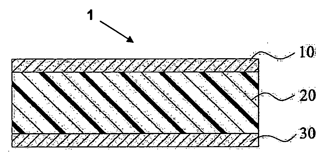
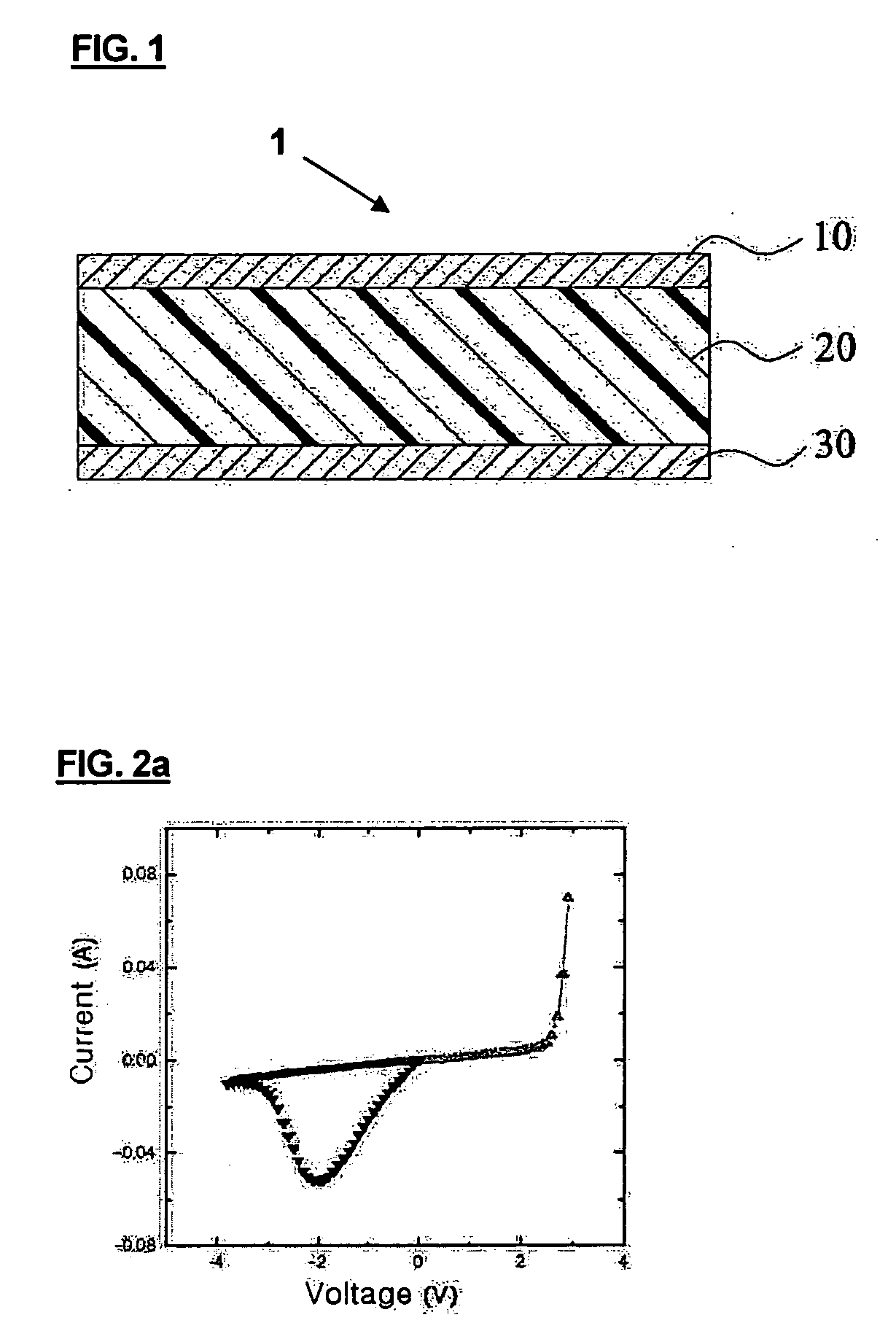
Nonvolatile nanochannel memory device using mesoporous material
a mesoporous material, non-volatile technology, applied in the direction of nanotechnology, semiconductor devices, electrical devices, etc., can solve the problems of increasing process costs, inability to realize high capacity of silicon based devices thus manufactured, and inability to achieve high capacity. , to achieve the effect of excellent reproducibility and uniform performan
- Summary
- Abstract
- Description
- Claims
- Application Information
AI Technical Summary
Benefits of technology
Problems solved by technology
Method used
Image

Examples
example 1
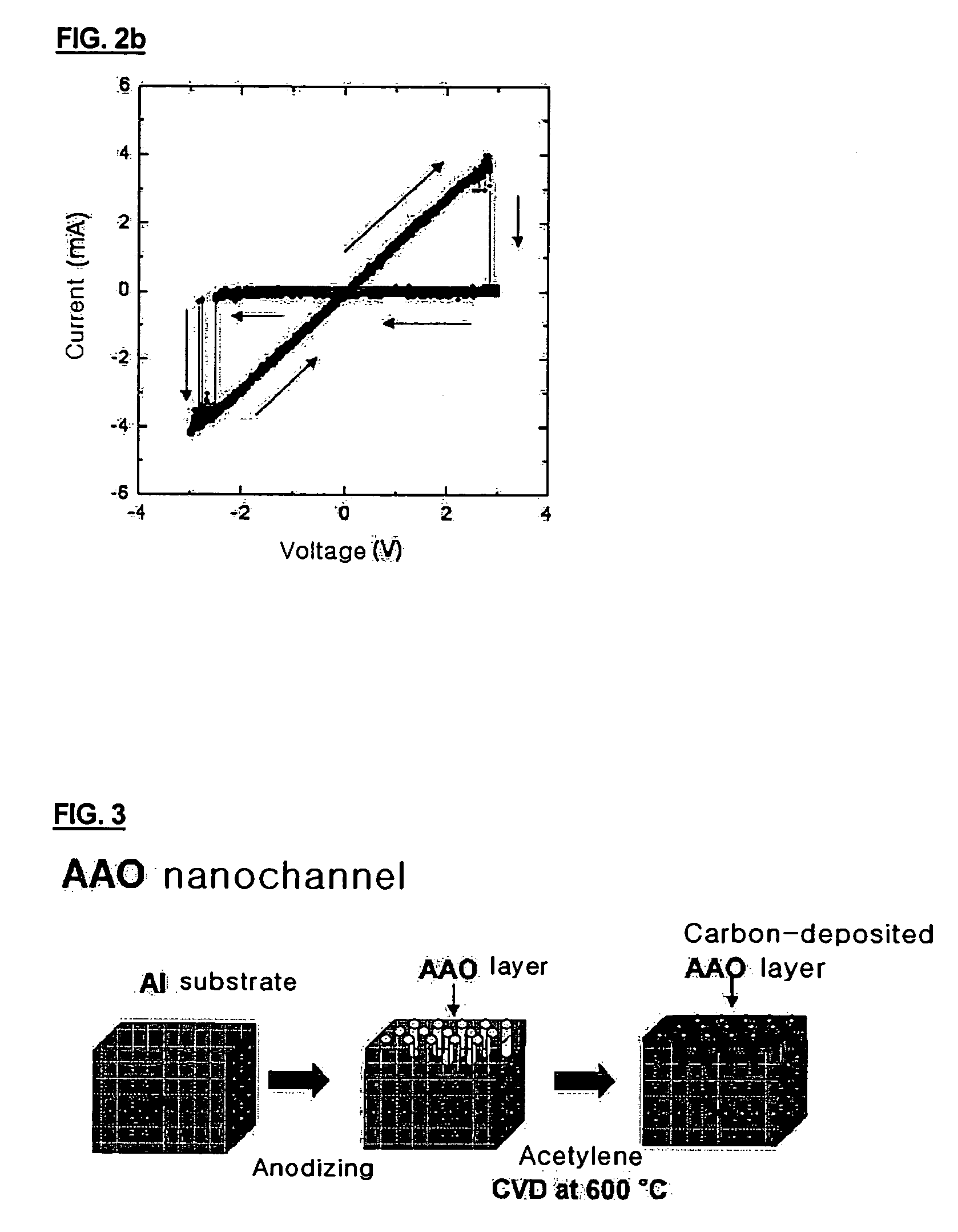
[0050] According to the process shown in FIG. 3, a memory device using anodized aluminum oxide (AAO) was manufactured as follows. Al was deposited to a thickness of 1000 nm on a 4″ Si wafer having SiO2 deposited to a 300 nm thickness, using an e-beam evaporator. Then, a reactor including sulfuric acid as an electrolyte and in which a platinum (Pt) plate was mounted as a cathode and the Al film cut to a suitable size was mounted as an anode, was stabilized at 0° C. The voltage of 25 V was applied to the above reactor, and anodic oxidation occurred for 8 min.
[0051] The AAO / Al film thus obtained was completely washed with distilled water, and then dipped into an etching solution comprising phosphoric acid and chromic acid mixed at 1.6:1.8 at 60° C. for 20 min, to remove the upper AAO layer. The etched Al film was loaded into an anodizing reactor, to which 25 V were applied, and the anodic oxidation took place for 8 min, to obtain a 500 nm thick AAO film.
[0052] On the AAO film thus ob...
example 2
[0055] As in the structure shown in FIG. 7, pores were formed using TiO2, which were then formed into nanochannels, after which a memory device was manufactured according to the following procedures.
[0056] 4.3 g of Ti(OEt)4 and excess deionized water were loaded into a 50 ml centrifuge tube, and then stirred and hydrated in the form of particles. Centrifuging was performed at 4000 rpm for 5 min, and water as a supernatant was decanted. Subsequently, the hydrated titanium particles were allowed to stand at room temperature for 5 min and then washed with excess acetone. After upper acetone was removed, white powdered hydrated titanium particles were sufficiently dried at room temperature, added with 2.6 g of concentrated HCl, and stirred at room temperature for 30 min, to obtain a transparent titanium hydroxide sol precursor.
[0057] 0.8 g of P123 (available from BASF), typically represented by an amphiphilic surfactant, and 10 g of ethanol were mixed, loaded into a 20 cc glass vial, ...
PUM
| Property | Measurement | Unit |
|---|---|---|
| size | aaaaa | aaaaa |
| thickness | aaaaa | aaaaa |
| size | aaaaa | aaaaa |
Abstract
Description
Claims
Application Information