Nonvolatile semiconductor memory device

a semiconductor and memory device technology, applied in semiconductor devices, digital storage, instruments, etc., can solve the problems of excessive extraction of electrons, erroneous reading, and need to consider “over-erasure” and other problems, to achieve the effect of low current consumption and high speed

Active Publication Date: 2006-11-02
RENESAS ELECTRONICS CORP
View PDF3 Cites 14 Cited by
  • Summary
  • Abstract
  • Description
  • Claims
  • Application Information

AI Technical Summary

Benefits of technology

[0013] An object of the present invention is to provide a nonvolatile semiconductor memory ...

Problems solved by technology

When the injection/extraction of electrons is performed on the floating gate to store data, a problem of “over-erasure” needs to be considered.
However, when the non-selected memory cell is in the over-erasure state, the current flows through this non-selected memory cell, and, there arises a problem that the data is determined based on a combined current of the selected memory cell and the non-selected memory cell in the over-erasure state in the sense amplifier, resulting in erroneous reading.
Thus, when the electrons are extracted from the floating gate to set a threshold voltage to a low state, there is possibility that a memory cell transistor from which the electrons are excessively extracted is produced even under the same voltage applying condition, so that the memory cell transistor in the over-erasure state is present.
Consequently, in order to prevent such over-erasure, the threshold voltage of the memory cell transistor can not be set sufficiently low, and thus, the problem arises that the data cannot be read under a low power supply voltage.
However, when the erasure verification operation is performed for each bit to control the threshold voltage distribution, the processing takes a long time and the processing ...

Method used


Image

  • Nonvolatile semiconductor memory device
  • Nonvolatile semiconductor memory device
  • Nonvolatile semiconductor memory device

Examples


embodiment 1

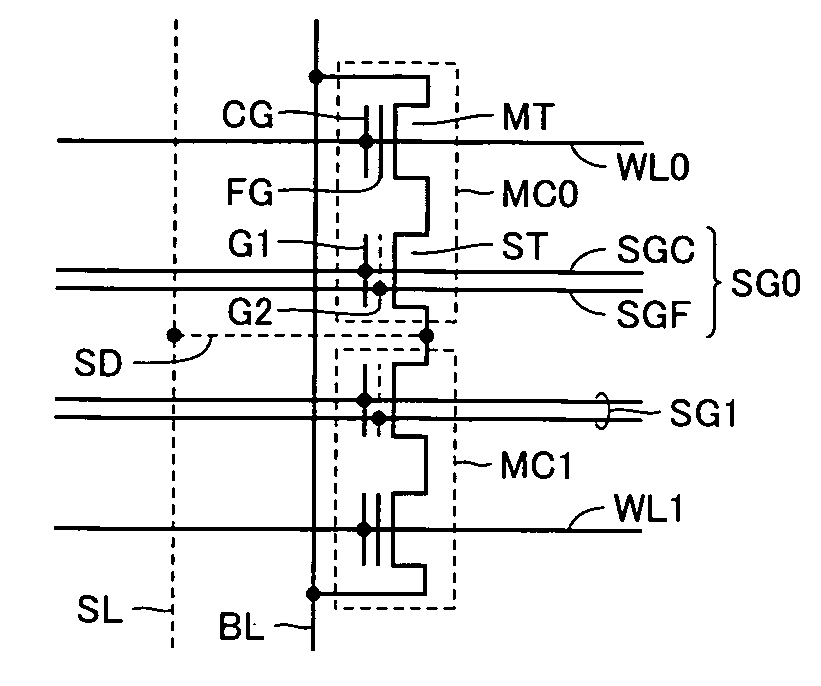
[0063]FIG. 1 is a diagram showing an electrical equivalent circuit of memory cells according to Embodiment 1 of the present invention. In FIG. 1, memory cells MC0 and MC1 of two bits are shown representatively. Since memory cells MC0 and MC1 have the same construction, reference numerals are allotted to components of memory cell MC0 in FIG. 1. Memory cell MC0 includes a memory transistor MT and a selection transistor ST which are connected in series between a bit line BL and a source line SL. Memory transistor MT includes a floating gate FG that stores information in the form of electric charges and a control gate CG formed above floating gate FG and connected to a word line WL0. Control gate CG is used to refer to a gate electrode arranged for each individual memory cell and word line WL (WL0, WL1) is used to refer to an interconnection line arranged extending continuously in a row direction for one row of memory cells and connecting to the control gates of the memory cell transist...

embodiment 2

[0177]FIG. 25 is a diagram schematically showing a construction of a nonvolatile memory cell array according to Embodiment 2 of the present invention. In FIG. 25, memory cells MC0 to MC3 of four bits disposed in alignment in one column are representatively shown. These memory cells MC0 to MC3 are connected to bit line BL in common and are connected to source line SL in common. These memory cells MC0 to MC3 are connected between bit line BL and source line SL in parallel each other.

[0178] Each of memory cells MC0 to MC3 has a three-layered gate structure and includes floating gate FG, and first and second control gate electrodes CG1 and CG2. For these memory cells MC0 to MC3, word lines WL0 to WL3 are arranged, respectively. Each of word lines WL0 to WL3 is connected to the memory cells arranged in alignment in one row in common.

[0179] Each of word lines WL0 to WL3 includes a word control line WCL and a word selection line WSL coupled to first and second control gate electrodes CG1...

embodiment 3

[0215]FIG. 33 is a diagram schematically showing a construction of a main portion of a nonvolatile semiconductor memory device according to Embodiment 3 of the present invention. In FIG. 33, a bottom N well 92 is provided in a circumference (outer periphery) of a p-type well 90. In p-type well 90, memory cells MC are formed, and word lines, bit lines and source lines are arranged corresponding to the memory cells. Namely, p-type well 90 is used for forming the memory cells.

[0216] Memory cell MC may be a stacked gate transistor having a floating gate (FG), or may be configured to have a charge trap film (ONO film). The floating gate and the charge trap film are collectively referred to as an electric charge accumulation region.

[0217] To bottom N well 92A, a well voltage Vnw from a bottom voltage generating circuit 94 is supplied, and to p-type well 90, a well voltage (substrate voltage) Vpw from a well voltage generating circuit 96 is supplied.

[0218]FIG. 34 is a diagram schematica...


PUM


Abstract

In a nonvolatile memory cell, a selection transistor is connected to a memory cell transistor in series. The selection transistor is formed into a double layer gate structure, and has a voltage of each gate driven individually and separately. Using capacitive coupling between these stacked gate electrode layers of the selection transistor, a gate potential of the selection transistor is set to the predetermined voltage level. An absolute value of the voltage level generated by a voltage generator to the gates of the selection transistor can be made small, so that current consumption can be reduced and an layout area of the voltage generator can be reduced. Thus, a nonvolatile semiconductor memory device with a low current consumption and a small chip layout area is provided.

Description

BACKGROUND OF THE INVENTION [0001] 1. Field of the Invention [0002] The present invention relates to a nonvolatile semiconductor memory device and particularly to a nonvolatile semiconductor memory device integrated on a common same semiconductor substrate (chip) with a logic circuit such as a processor. More specifically, the present invention relates to a construction for reducing power consumption and occupying area of the nonvolatile semiconductor memory device and for reading data at high speed. [0003] 2. Description of the Background Art [0004] Semiconductor memory devices that store information in a nonvolatile manner include a flash memory. In the flash memory, a memory cell is formed of one stacked gate field effect transistor (memory cell transistor) having a floating gate. An electric field is applied to the floating gate to perform injection / extraction of electric charges (electrons) on the floating gate through an F-N (Fowler-Nordheim) tunneling phenomenon or a Channel ...

Claims


Application Information

Patent Timeline
IPC IPC(8): G11C16/04G11C11/34
CPCG11C16/344G11C16/3445H01L27/11529G11C16/3477H01L27/11526G11C16/3468H10B41/41H10B41/40
Inventor ISHII, MOTOHARUENDO, SEIICHI
Owner RENESAS ELECTRONICS CORP
Why Eureka
Try Eureka