Method and apparatus for the production of silicon carbide crystals

a technology of silicon carbide crystals and manufacturing methods, applied in the direction of crystal growth process, polycrystalline material growth, under a protective fluid, etc., can solve the problems of reducing the breakdown voltage of the sic device, undesirable affecting the device characteristics, current leakage, etc., to reduce the concentration of defects, and reduce the defect concentration

Active Publication Date: 2006-11-16
CREE INC
View PDF11 Cites 40 Cited by
  • Summary
  • Abstract
  • Description
  • Claims
  • Application Information

AI Technical Summary

Benefits of technology

[0012] The present invention provides a method and apparatus for the production of silicon carbide crystalline materials having reduced defects. To reduce the concentration of defects, silicon carbide crystals are grown in alternating crystallographic growth directions. Alternating the growth of silicon carbide in this manner can terminat...

Problems solved by technology

For example, crystal imperfections in the SiC single crystal, including micropipe defects, screw dislocations, edge dislocations, stacking faults, and the like, can result in current leakage and reduced breakdown voltage in a SiC device.
Accordingly, the defects and dislocations will also exist in the epitaxial layer at substantially the same density as in the SiC single crystal wafer and will undesirably affect device characteristics as well.
The resultant crystal, however, can include other undesired defects, primarily stacking faults located on {0001...

Method used


Image

  • Method and apparatus for the production of silicon carbide crystals
  • Method and apparatus for the production of silicon carbide crystals

Examples


Embodiment Construction

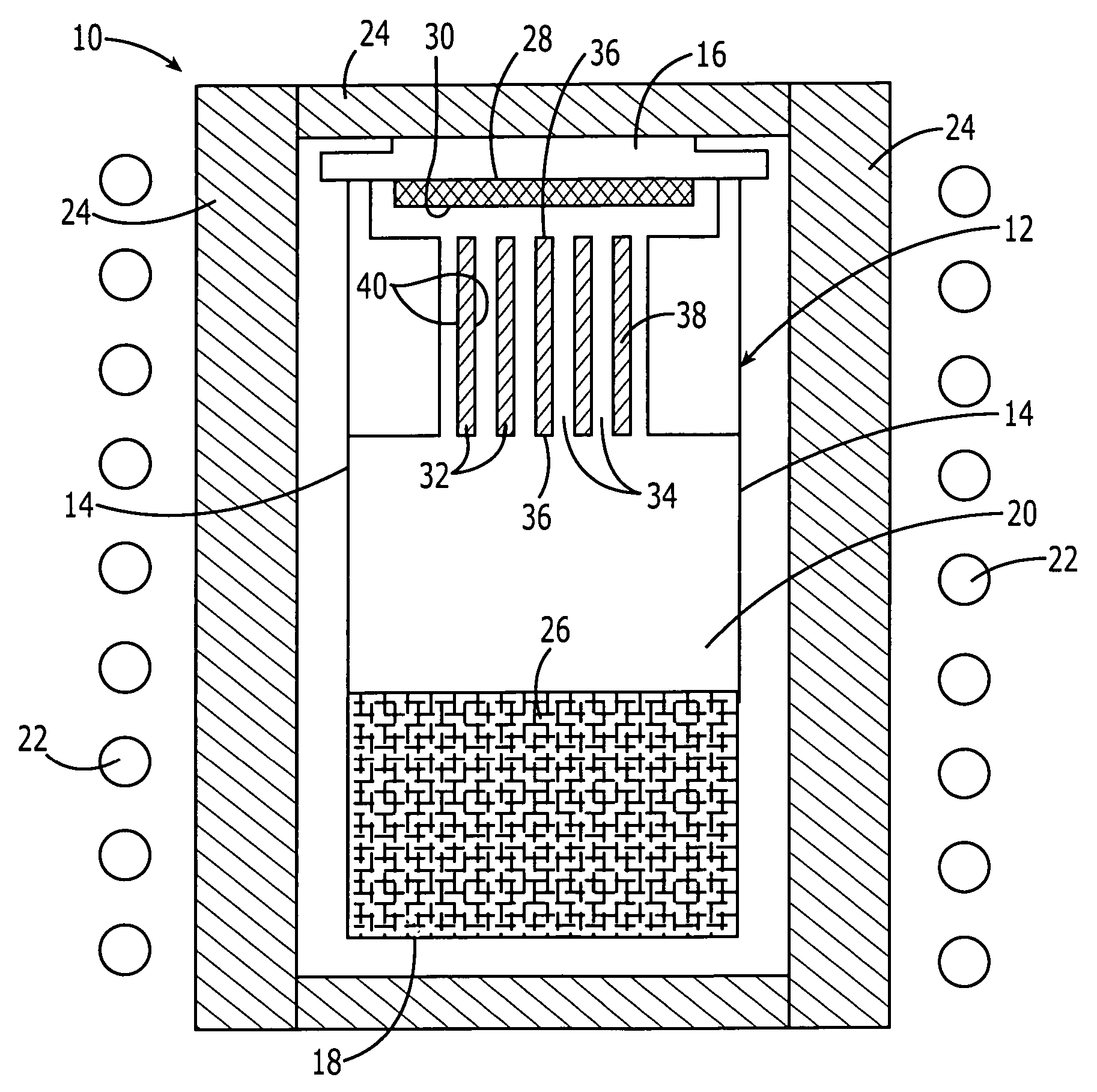
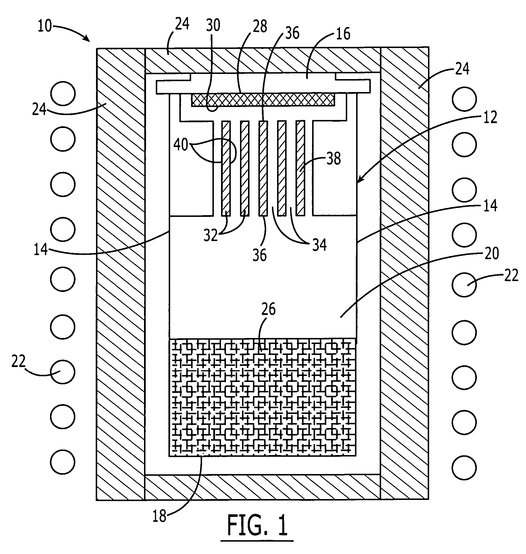
[0021] The present invention now will be described more fully hereinafter with reference to the accompanying drawing, in which some, but not all embodiments of the invention are shown. Indeed, this invention may be embodied in many different forms and should not be construed as limited to the embodiments set forth herein; rather, these embodiments are provided so that this disclosure will satisfy applicable legal requirements. Like numbers refer to like elements throughout.

[0022] The general aspects of various techniques for the growth of silicon carbide, including chemical vapor deposition and seeded sublimation techniques, have been generally well established for a number of years. Furthermore, those familiar with the growth of crystals, particularly in difficult material systems such as silicon carbide, will recognize that the details of a given technique can and will vary, usually purposefully, depending upon the relevant circumstances. Accordingly, descriptions given herein ar...


PUM


Abstract

A method and apparatus for growing silicon carbide crystals is provided. The apparatus includes a sublimation chamber with a plurality of spaced apart dividers that can direct the direction of silicon carbide crystal growth into passages between the dividers to form a plurality of silicon carbide crystal plates. The silicon carbide crystal plates can be used as seed crystals in subsequent sublimation steps in a manner that promotes the growth of silicon carbide crystals in different crystallographic directions to thereby terminate defect formation.

Description

BACKGROUND OF THE INVENTION [0001] The present invention relates to a method and apparatus for the manufacture of silicon carbide crystalline material. [0002] Silicon carbide (SiC) is a desired material for use in the manufacture of semiconductor devices. Silicon carbide has a variety of properties useful in such devices, including a wide bandgap, a high thermal coefficient, a low dielectric constant and high temperature stability. As a result, silicon carbide materials can provide excellent semiconducting properties, and electronic devices made from silicon carbide can perform at higher temperatures as compared to devices made from other materials currently used in the industry. [0003] Traditionally, two broad categories of techniques have been used for forming crystalline silicon carbide for semiconductor applications. The first of these techniques is known as chemical vapor deposition (“CVD”) in which reactant gases are introduced into a system to form silicon carbide crystals, t...

Claims


Application Information

Patent Timeline
IPC IPC(8): C30B23/00C30B28/12
CPCC30B23/00C30B35/00Y10T117/1068Y10T117/1052Y10T117/1032C30B29/36
Inventor TSVETKOV, VALERI F.MALTA, DAVID P.
Owner CREE INC
Why Eureka
Try Eureka