Light emitting diode and manufacturing method thereof

a technology of light-emitting diodes and manufacturing methods, which is applied in the direction of basic electric elements, electrical equipment, semiconductor devices, etc., can solve the problems of difficult growth of gan-based materials on a flat surface, high light extraction efficiency, and low production cost of low-cost electrode pads. achieve the effect of improving light extraction efficiency and avoiding the adverse effect of low-cost electrode pads

Inactive Publication Date: 2006-12-07
SUMITOMO CHEM CO LTD
View PDF11 Cites 51 Cited by
  • Summary
  • Abstract
  • Description
  • Claims
  • Application Information

AI Technical Summary

Benefits of technology

[0047] The object of the present invention is to provide a technique of ensuring compatibility between the method of improving the light extraction efficiency by roughening the surface of the LED structure, and the method of avoiding the adverse effect of a low-cost electrode pad ((1) forming a current distribution layer by the transparent conductive film made of metal or metal oxide, and (2) forming a flip chip structure).
[0054] As described above, a concavo-convex pattern is formed on the surface of the semiconductor lamination structure. Not only that, a flat portion is maintained on the surface of the semiconductor lamination structure, thereby preventing the p-type semiconducting layer from being turned into the n-type semiconducting layer by the aforementioned doping, and avoiding high contact resistance.
[0055] The active layer is composed of 30 or less quantum well layers, whereby re-absorption of light on the active layer is reduced and effective improvement of the light extraction efficiency is ensured. Further, the depth of the bore is kept smaller than the distance between the active layer and flat portion, thereby preventing occurrence of a short circuit between the electrode and light emitting area (active layer).
[0058] As described above, a transparent conductive film is formed on the surface of the semiconductor lamination structure with the flat portion maintained. This structure prevents the transparent conductive film from being divided into sections to cause current distribution failure, when a transparent conductive film is formed on the surface of the semiconductor lamination structure.
[0128] As described above, a concavo-convex pattern is formed on the surface of the semiconductor lamination structure. Not only that, a flat portion is maintained on the surface of the semiconductor lamination structure, thereby preventing the p-type semiconducting layer from being turned into the n-type semiconducting layer by the aforementioned doping, and avoiding high contact resistance. The active layer is composed of 30 or less quantum well layers, whereby re-absorption of light on the active layer is reduced and effective improvement of the light extraction efficiency is ensured.
[0130] The present invention provides a technique of ensuring compatibility between the method of improving the light extraction efficiency by roughening the surface of the LED structure, and the method of avoiding the adverse effect of a low-cost electrode pad ((1) forming a current distribution layer by the transparent conductive film made of metal or metal oxide, and (2) forming a flip chip structure).

Problems solved by technology

To put it another way, on the active layer of the LED structure, light is emitted in all directions, but much of the light having been generated cannot be extracted to the outside of the LED due to the full reflection on the LED structure surface.
It is repeatedly subjected to full reflection and is absorbed during this process, and is lost in the form of heat by recombination through a defect level.
For the GaN-based LED, growth of a GaN-based material on a flat surface was difficult in the stage of the Patent Document 1 or in the initial stage of the study of the GaN-based LED prior to the Patent Document 1.
Thus, the light extraction efficiency cannot be improved despite the efforts of roughening the surface and converting the light reflection angle.
Such an electrode pad does not allow the passage of light, and prevents light from being extracted out of the device.
Since the thickness of the current distribution layer is much greater than that of the active layer (typically 1 μm or less), there will be an increase in the thickness of the grown film, accompanied by greater production costs.
In addition to this disadvantage, since such a current distribution layer is normally doped to a high density, light is absorbed by the defect level caused by impurity level and high-density doping.
If the thickness is as much as 10 μm, there will a substantial reduction in efficiency due to light absorption.
However, serious difficulties follows in most cases when the aforementioned (1) or (2) and the method of roughening the surface of the LED is used in combination in practice.
This makes it difficult to form a thin transparent conductive film over the entire surface, without dividing it into sections.
This is accompanied by excessive absorption of light by the Mg doped GaN or Si-doped GaN layer, and the light extraction efficiency is reduced by any of the aforementioned methods (1) and (2), against expectation.
Thus, it is impossible to achieve continuous formation of a transparent conductive film when using the surface configuration shown in FIGS.
In this case, current cannot be distributed over the entire surface, with the result that the light emitting capacity of the LED cannot be improved effectively.
As described above, a technique has not yet been established to ensure compatibility between the method of improving the light extraction efficiency by roughening the surface of the LED structure, and the method of avoiding the adverse effect of a low-cost electrode pad ((1) forming a current distribution layer by the transparent conductive film made of metal or metal oxide, and (2) forming a flip chip structure).
The problems that occur in joint use of the method of roughening the surface and the method of the aforementioned (1) and (2) also arise in other semiconductors.

Method used


Image

  • Light emitting diode and manufacturing method thereof
  • Light emitting diode and manufacturing method thereof
  • Light emitting diode and manufacturing method thereof

Examples


embodiment 1

[0149] The method of manufacturing the prior art light emitting diode (LED) as a basis will be first described with reference to FIGS. 15 and 16.

[0150] According to the MOVPE method, a LED structure emitting blue light was grown on a substrate (501 or 601), having a diameter of 2 inches, composed of a sapphire with surface C. To put it more specifically, a substrate (501 or 601) composed of sapphire was put into a MOVPE apparatus. Then it was heated in the atmosphere of a nitrogen / hydrogen mixed gas of 760 Torr (overall flow rate=150 slm; nitrogen / hydrogen=2) at 1135 degrees Celsius for 10 minutes, whereby the oxides were removed from the surface of the substrate (by thermal cleaning).

[0151] After that, the substrate temperature was reduced to 515 degrees Celsius. At the same time, the flow rate of the carrier gas was set at 140 slm and volume ratio of nitrogen / hydrogen in the carrier gas was set at 1.5. Under this condition, ammonia (NH3) gas as a nitrogen material was put into t...

embodiment 2

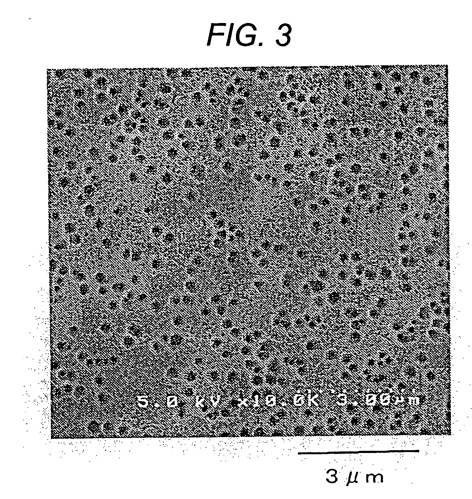
[0176] In the LED structure of the first embodiment, epitaxial wafers were manufactured wherein the number of undoped In0.15Ga0.85N layers in the InGaN / GaN multiple quantum well layer (active layer) (105, 205) is 1 through 50. A prior art surface light extraction type LED structure and a surface light extraction type LED structure having bores were formed on the surface in the manner similar to the first embodiment were manufactured from each epitaxial wafer.

[0177]FIG. 4 shows the number of the quantum well layers and the rate of output increase (the maximum light emitting output obtained from the LED structure with bores formed on the surface / outputted light emitting output of the prior art LED structure) resulting from formation of bores on the surface. As shown in FIG. 4, when the number of the quantum well layers is more than 30, the light emitting output is not increased even if bores are formed on the surface (the rate of output increase: 1 or less).

[0178] This is due to an ...

embodiment 3

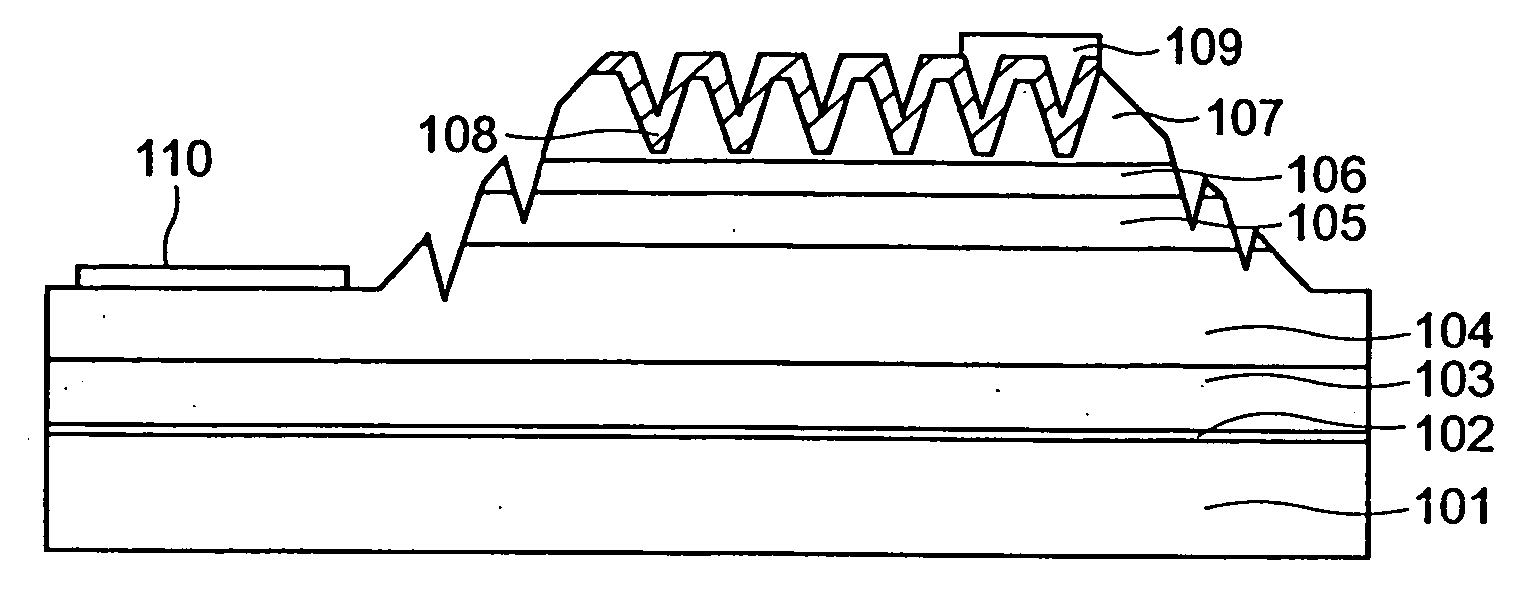
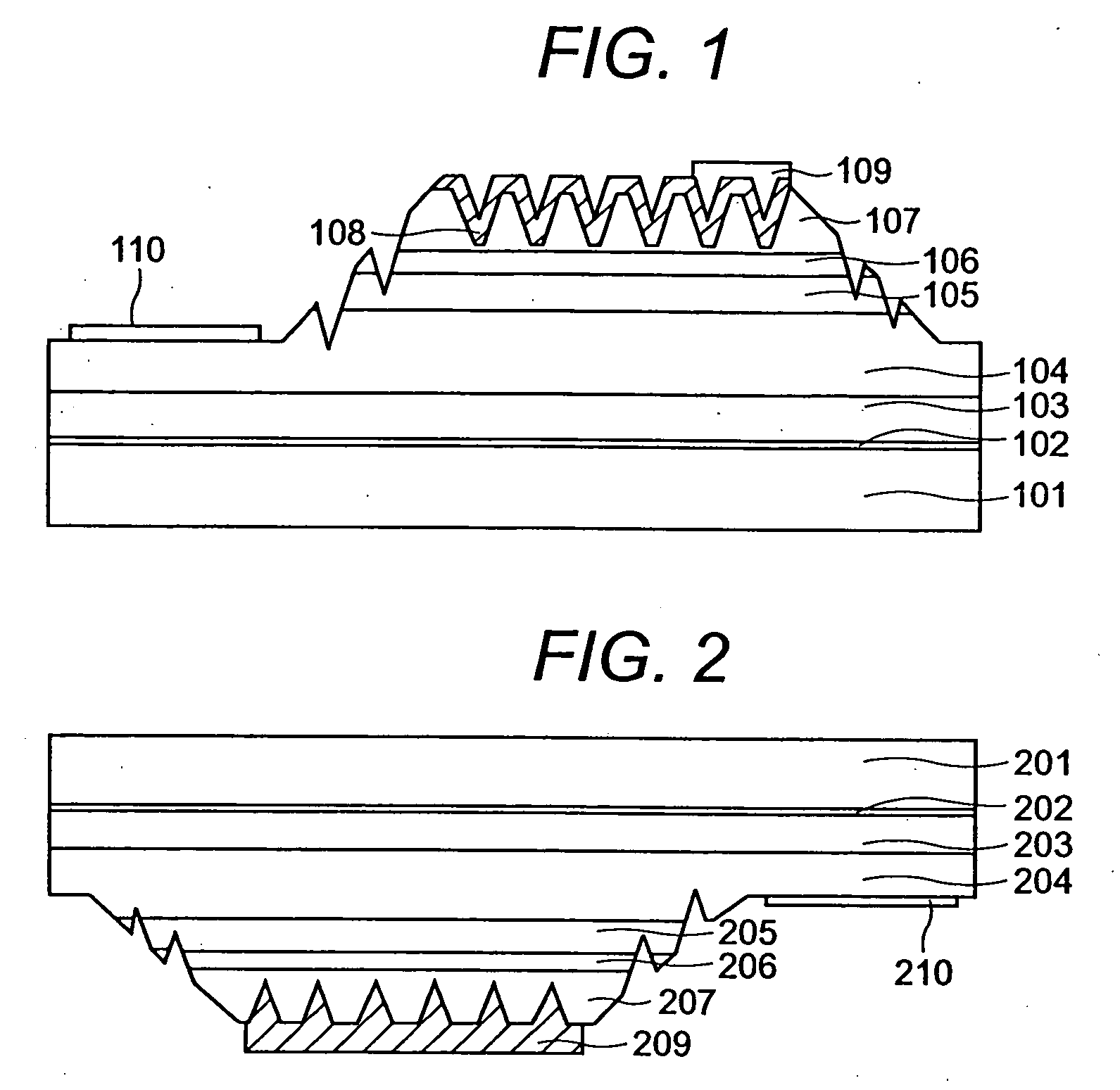
[0179] As shown in FIGS. 5 and 6, in the LED structure of the first embodiment, a Si doped n-type Al0.1Ga0.9N layer (111, 211) having a Si density of 3×1018 cm−3 was inserted between the n-type GaN layer (104, 204) and InGaN / GaN multiple quantum well layer (active layer) (105, 205).

[0180] An epitaxial wafer for a blue-violet LED (emitted light wavelength: 400 nm) was manufactured, wherein the active layer of this blue-violet LED was an InGaN / GaN multiple quantum well layer (active layer) (105, 205), this InGaN / GaN multiple quantum well layer being composed of a 6-cycle, Si doped n-type GaN layer having a density of undoped In0.06Ga0.94N (film thickness: 3.5 nm) / Si of 3×1018 cm−3.

[0181] Then the same experiment as that in the first embodiment was conducted. Similarly to the case of the first embodiment, a considerable increase was observed in the light emitting output over the prior art LED structure under the following conditions:

[0182] 1) The percentage of the area occupied by t...


PUM


Abstract

A technique of ensuring compatibility between the method of improving the light extraction efficiency by roughening the surface of a LED structure, and the method of avoiding the adverse effect of a low-cost electrode pad ((1) forming a current distribution layer by a transparent conductive film made of metal or metal oxide, and (2) forming a flip chip structure). A light emitting diode comprises at least an n-type semiconducting layer, an active layer composed of 30 or less quantum well layers, and a p-type semiconducting layer provided on a substrate, wherein the surface of the semiconductor lamination structure contains a flat portion and a plurality of bores. In this case, the in-plane coverage rate ((the area of the bore opening / surface area)×100) of the plurality of the bores is 10% or more without exceeding 85%; the opening of the bore has a diameter of 100 nm or more without exceeding 4000 nm; the depth of the bore is smaller than the distance between the active layer and the flat portion; and the density of the plurality of the bores expressed in terms of number of bores is 8×10⁵ per / cm2 or more without exceeding 1.08×10¹⁰ per / cm2.

Description

BACKGROUND OF THE INVENTION [0001] 1 Field of the Invention [0002] The present invention relates to a light emitting diode (LED) and manufacturing method thereof capable of providing excellent effects in internal quantum efficiency and light extraction efficiency over the prior art. [0003] 2. Background of the Invention [0004] Efficiency is one of the most important percentage indices in the LED. To be more specific, the LED is required to provide a high light emitting efficiency with the least possible current, namely, to provide high efficiency. [0005] Generally, efficiency depends on the internal quantum efficiency and light extraction efficiency. The internal quantum efficiency can be defined as opto-electrical conversion efficiency in the LED, namely, the efficiency wherein the injected current is converted into photon in the light emitting layer. [0006] The light extraction efficiency refers to the efficiency wherein the light produced in the light emitting layer is extracted ...

Claims


Application Information

Patent Timeline
Patent Type & Authority Applications(United States)
IPC IPC(8): H01L29/22H01L33/06H01L33/32H01L33/38H01L33/42
CPCH01L33/20H01L33/22H01L33/42H01L33/382H01L33/24
Inventor FUJIKURA, HAJIMENAKAYAMA, SATOSI
Owner SUMITOMO CHEM CO LTD
Why Eureka
Try Eureka