Eureka AIR delivers breakthrough ideas for toughest innovation challenges, trusted by R&D personnel around the world.

Process for producing extremely flat microcrystalline diamond thin film by laser ablation method

a laser ablation and diamond thin film technology, applied in the direction of crystal growth process, solid state diffusion coating, polycrystalline material growth, etc., can solve the problem of future coating and electronic device application difficulties

Inactive Publication Date: 2007-01-25
JAPAN SCI & TECH CORP
View PDF3 Cites 9 Cited by
  • Summary
  • Abstract
  • Description
  • Claims
  • Application Information

AI Technical Summary

Benefits of technology

[0024] An extremely small target-substrate distance, namely 15 to 25 mm, provides a higher degree of supersaturation of supersaturated carbon, which is essential for the growth of diamond in a high-temperature, high-pressure phase. Such a small distance also causes high-energy carbon particles emitted from the target to collide with atmospheric hydrogen, which then dissociates into atomic hydrogen. As a result, excited carbon atoms and molecules and atomic hydrogen occur in an ablation plume surrounding the substrate. This allows a simultaneous supply of supersaturated carbon and hydrogen for the growth of diamond on the substrate.
[0025] Atomic hydrogen has been found to have two effects. One of them is the effect of selectively etching off sp2 bond fractions (graphite fractions), though the effect is weaker than that of oxygen. The pressure of the hydrogen is preferably about 2 to 10 Torr for an extremely small target-substrate distance, namely 15 to 25 mm, because of the weaker effect (for oxygen, a pressure of 50 to 70 mTorr is preferred).
[0026] The other is the effect of linking diamond crystal grains to facilitate the growth of a continuous film. When diamond starts growing on a substrate in a supersaturated state of carbon, atomic hydrogen intrudes between diamond crystal grains so as to link them. The atomic hydrogen moves to the surface of the film at the stage where the diamond crystals grow while combining with each other, so that substantially no atomic hydrogen remains in the film. That is, the atomic hydrogen acts as a surfactant. For CVD, hydrogen originating mainly from CH4 remains in resultant films. Such residual hydrogen decreases the optical transmittance and hardness of the films, degrading the quality of the films. Thus, the advantage of leaving less atomic hydrogen is preferred for the growth of high-quality films. If the supersaturated state is not achieved because of a large target-substrate distance, the atomic hydrogen combines with carbon atoms to form hydrogenated amorphous carbon.
[0027] While films that are composed of crystal grains and are discontinuous in a plane are produced according to reports that have so far been made, the process according to the present invention enables the growth of a continuous, single-phase nanocrystalline diamond film by means of the above two effects. The resultant film is ultraflat with a surface roughness of about 1 nm or less. In addition, the film contains substantially no non-diamond component. In Raman spectrometry, the film exhibits only a sharp peak at 1,333 cm−1, which is attributed to diamond. Furthermore, the film can be allowed to grow at ultrahigh speed, namely about 4 μm / hour or more. Table 1 shows the properties of nanocrystalline diamond in comparison with those of diamond-like carbon, polycrystalline diamond, and single-crystal diamond. TABLE 1NanocrystallinePolycrystallineSingle-crystalDiamond-like carbondiamonddiamonddiamondAmorphousNanocrystalPolycrystalSingle crystalGrowth on foreignEasyPossibleDifficultExtremelysubstratedifficultStability againstDeteriorate withStableStableStabletemperaturetemperature becauseof nonequilibriumphaseBandgapVary below 5.6 eV5.6 eV5.6 eV5.6 eVdepending on sp2-to-sp3 ratioInsulationGoodGoodGoodExcellentFilm flatnessFlatFlatIrregularFlatSmoothnessExcellentExcellentExcellentFairThermal conductivityPoorExcellentExcellentExcellentTransmittanceGoodExcellentExcellentExcellentPotential asPoorGoodGoodFairsemiconductoroperable at hightemperaturePotential as coatingExcellentExcellentFairPoormaterialPotential as heat sinkPoorExcellentFairPoormaterial
[0029] On the other hand, single-crystal diamond and polycrystalline diamond are difficult to produce. Even if they can be produced, they often contain gaps between crystal grains and tend to form irregular, discontinuous films. Nanocrystalline diamond can overcome such problems without substantially impairing the other advantages of diamond.
[0030] Ultraflat, single-phase diamond films are demanded for future application to devices. Ultraflat nanocrystalline diamond films can be allowed to grow at ultrahigh speed using hydrogen as an atmospheric gas at high hydrogen atmosphere pressure by reducing a target-substrate distance.

Problems solved by technology

The resultant film, however, includes diamond crystal grains with a size of about 1 μm and has an irregular surface, and thus has difficulty in being applied to electronic devices and coatings in future.

Method used


Image

  • Process for producing extremely flat microcrystalline diamond thin film by laser ablation method
  • Process for producing extremely flat microcrystalline diamond thin film by laser ablation method
  • Process for producing extremely flat microcrystalline diamond thin film by laser ablation method

Examples


example 1

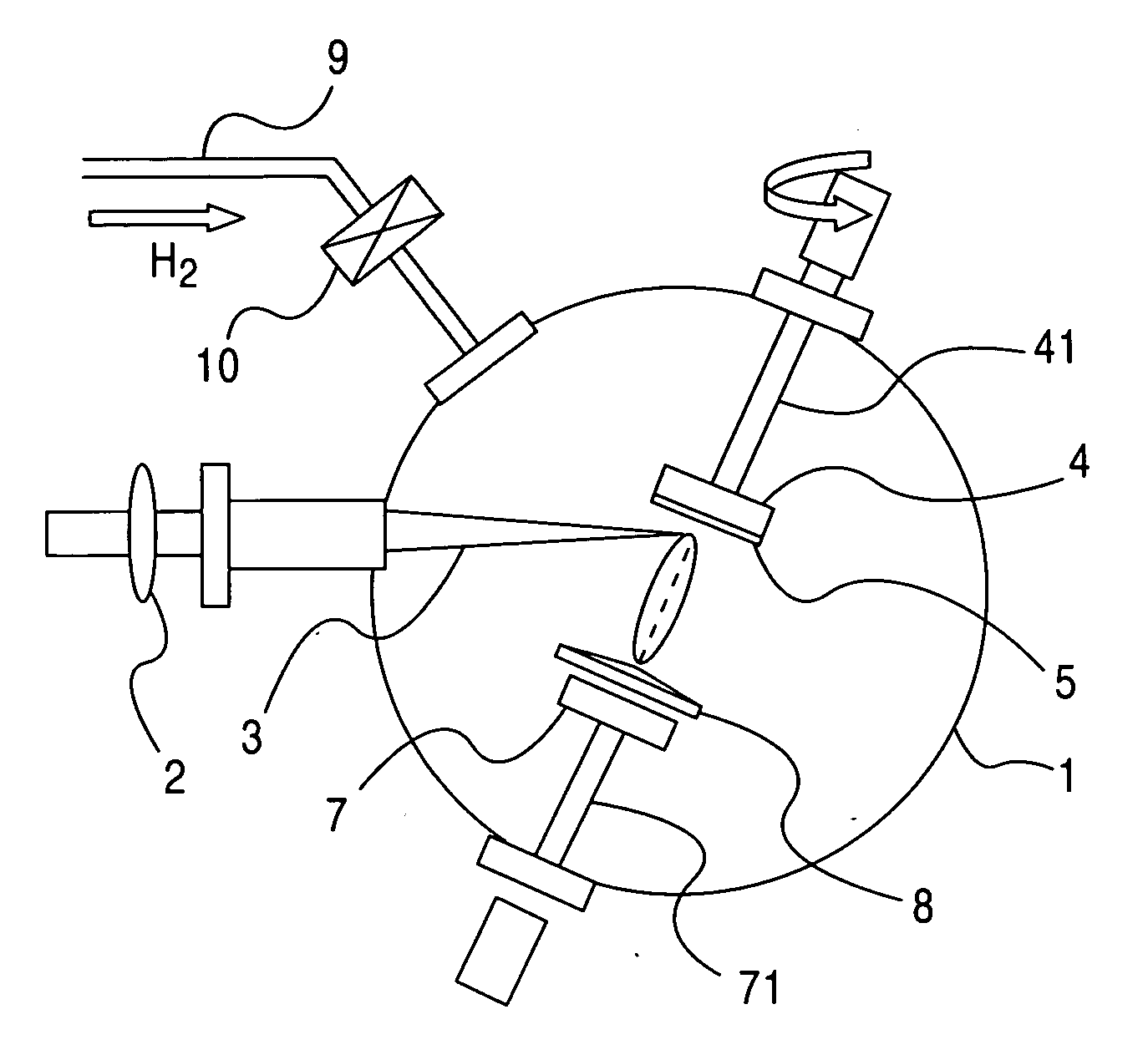
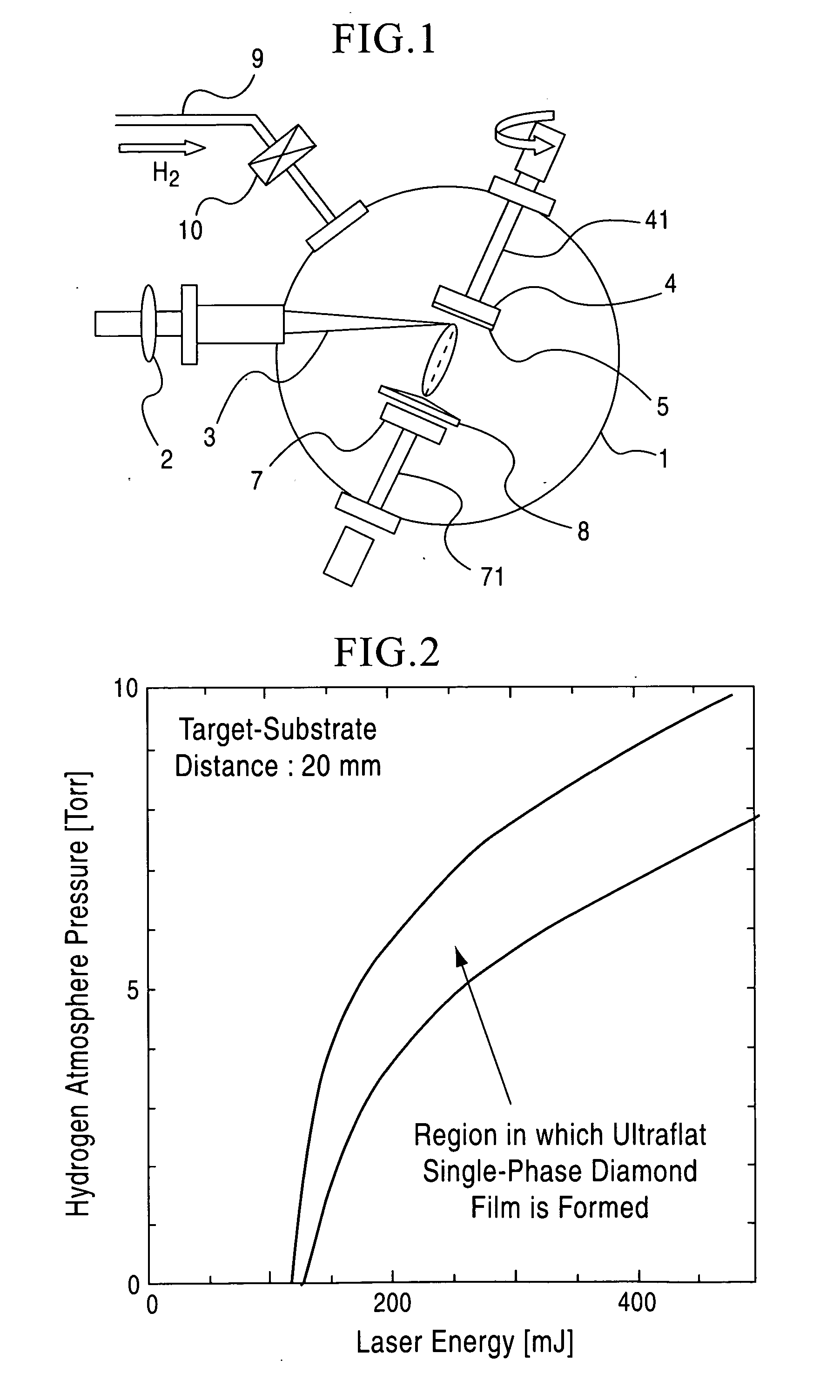
[0059] The hydrogen pressure was 4 Torr. For the hydrogen pressure, a film that was ultraflat over the surface was observed, as shown in FIG. 6. According to Raman spectrometry, only a shape peak at 1,333 cm−1, which is attributed to diamond, was observed, as shown in FIG. 7. These results indicate the growth of single-phase diamond containing substantially no non-diamond component.

[0060] A comparison of the SEM image in FIG. 6 with the SEM image in FIG. 8, which shows a diamond film produced using oxygen as an atmospheric gas, reveals that the film produced using hydrogen as an atmospheric gas was ultraflat. FIG. 9 shows an AFM image of the diamond film produced in Example 1. FIG. 10 shows a surface irregularity profile obtained by AFM measurement. A stripe pattern derived from the diamond substrate was observed. The average surface roughness was measured to be 2.2 nm; the film can be determined to be ultraflat at the atomic level with a roughness of about 1 nm or less without the...

example 2

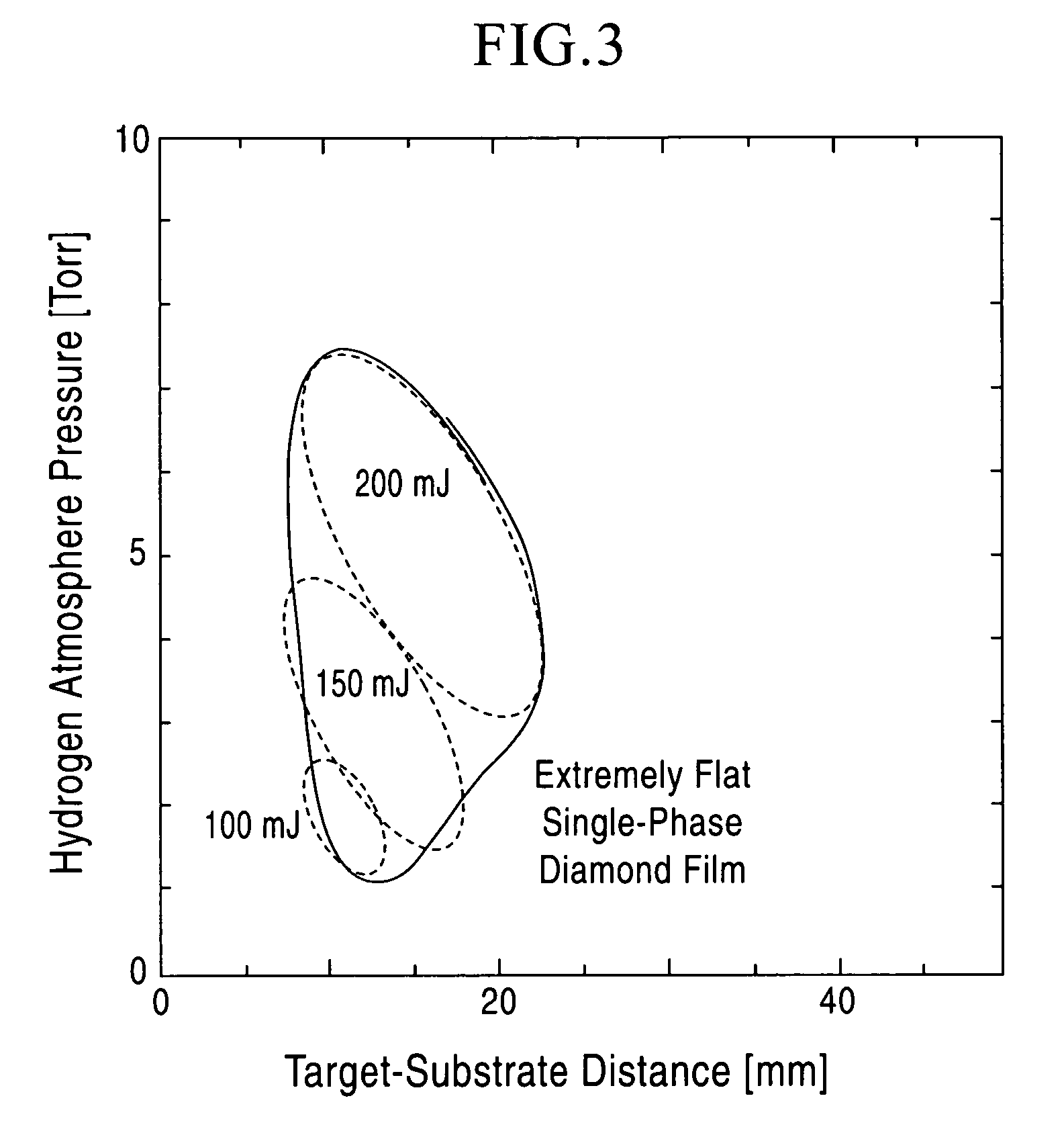
[0063] A continuous, ultraflat, single-phase nanocrystalline diamond thin film grew under the same conditions as in Example 1 except that the laser energy was 150 mJ, the target-substrate distance was 15 mm, and the hydrogen pressure was 2 Torr.


PUM

PropertyMeasurementUnit
Temperatureaaaaaaaaaa
Lengthaaaaaaaaaa

Abstract

Diamond thin films deposited by known PLD processes are composed of diamond crystal grains with a size of about 1 μm and have an irregular surface. A process for producing an ultraflat nanocrystalline diamond thin film by laser ablation includes creating atomic hydrogen and a supersaturated state of carbon in a space between a target and a substrate in a hydrogen atmosphere inside a reaction chamber at a substrate temperature of 450° C. to 650° C., a laser energy of 100 mJ or more, and a target-substrate distance of 15 to 25 mm to enable the growth of an ultraflat, single-phase nanocrystalline diamond thin film containing substantially no non-diamond component. The hydrogen atmosphere has a sufficient pressure to selectively completely etch off sp2 bond fractions (graphite fractions) deposited on the substrate with sp3 bond fractions remaining.

Description

TECHNICAL FIELD [0001] The present invention relates to processes for producing an ultraflat nanocrystalline diamond thin film by laser ablation (pulsed laser ablation), which is one of the physical vapor deposition methods. BACKGROUND ART [0002] Methods for producing thin films are broadly divided into physical vapor deposition (PVD) and chemical vapor deposition (CVD). Most studies on the deposition of diamond thin films are based on CVD, which has allowed the deposition of single-phase diamond films. Films achieved by known CVD methods, however, have a surface roughness of not less than 70 nm. Recent technology has succeeded in depositing ultraflat films with a surface roughness of about 1 nm or less and has reached the stage of examination for application to devices, though the growth of extremely flat films involves extremely low deposition rates, namely 20 to 30 nm / hour. For PVD, growth by sputtering or ion beam deposition has been attempted, though no continuous advances have...

Claims


Application Information

Patent Timeline
IPC IPC(8): C23C8/00C30B29/04C01B31/06C23C14/06C23C14/28C30B23/02
CPCC01B31/06C23C14/0611C23C14/28C30B23/02C30B29/04C01B32/25C01B32/26
Inventor YOSHITAKE, TSUYOSHINAGAYAMA, KUNIHITOHARA, TAKESHI
Owner JAPAN SCI & TECH CORP
Why Eureka
Eureka Blog
Learn More