Supercharge Your Innovation With Domain-Expert AI Agents!

Method for forming a capping layer on a semiconductor device

a technology of capping layer and semiconductor device, which is applied in the field of semiconductor devices, can solve the problems of inconvenient capping layer formation, inability to meet the requirements of the device, and relatively rough surface of cobalt film

Inactive Publication Date: 2007-03-01
FREESCALE SEMICON INC
View PDF6 Cites 6 Cited by
  • Summary
  • Abstract
  • Description
  • Claims
  • Application Information

AI Technical Summary

Benefits of technology

[0013] An active circuitry layer is formed on a substrate. The interconnect level is formed on top of the active circuitry level by depositing a dielectric layer and patterning the dielectric layer to form cavities, which can be vias, trenches, and the like. A diffusion barrier layer, such as tantalum or tantalum nitride, is deposited over the patterned dielectric layer such that the cavities and the top of the patterned dielectric layer are lined with the diffusion barrier layer. A conductive metal, such as copper, is deposited over the diffusion barrier layer, filling the cavities and forming a blanket film over the patterned dielectric layer. The diffusion barrier layer prevents diffusion of the conductive metal into the dielectric layer. The blanket film of the conductive metal is removed by chemical mechanical polishing (CMP) or other planarization method and the conductive metal remains in the cavities. The diffusion barrier layer is not substantially removed with the blanket film of the conductive metal, or in a separate planarization step, and remains on the surface of the patterned dielectric. This remaining diffusion barrier layer protects the dielectric layer from damage from further processing, such as CMP. The conductive metal remaining in the cavities is then recessed through selective chemical etching or deliberate dishing through CMP or other planarization process. The capping layer of cobalt or cobalt doped with other conductive elements is then deposited through electroless plating or other deposition process such that it overfills the recessed area above the conductive metal. The capping layer extending above the cavity and the barrier layer on top of the patterned dielectric layer is removed by a single CMP process or other planarization process. The surface roughness of the capping layer is reduced through this planarization process resulting in reduced leakage.
[0014] By leaving the diffusion barrier layer on top of the patterned dielectric layer after the conductive metal layer is removed, the dielectric surface is not exposed during the deposition of the capping layer or during a substantial portion of the simultaneous planarization of the capping layer and removal of the diffusion barrier layer. By not exposing the dielectric layer to the capping layer deposition process, diffusion of materials used in the capping layer deposition process is significantly reduced. In the case of electroless deposition of the capping layer, the remaining diffusion barrier layer substantially prevents the diffusion of metal ions into the dielectric layer resulting in reduced leakage caused by trapping of conductive materials. The remaining diffusion barrier layer also provides additional mechanical strength during the simultaneous planarization of the capping layer and substantial removal of the diffusion barrier layer resulting in reduced damage of the dielectric film. The benefits of reduced mechanical damage and reduced diffusion of contaminants into the dielectric layer are greater when the dielectric layer is a lower dielectric constant material. Furthermore, the method of forming the capping layer is simplified by planarizing the capping layer and removing the diffusion barrier layer remaining on the dielectric layer in one process step rather than in separate steps.

Problems solved by technology

The mushroom shape extends above the surface of the dielectric and may cause unacceptable leakage between conductors.
In addition, the plating process results in cobalt film with a relatively rough surface.

Method used


Image

  • Method for forming a capping layer on a semiconductor device
  • Method for forming a capping layer on a semiconductor device
  • Method for forming a capping layer on a semiconductor device

Examples


Embodiment Construction

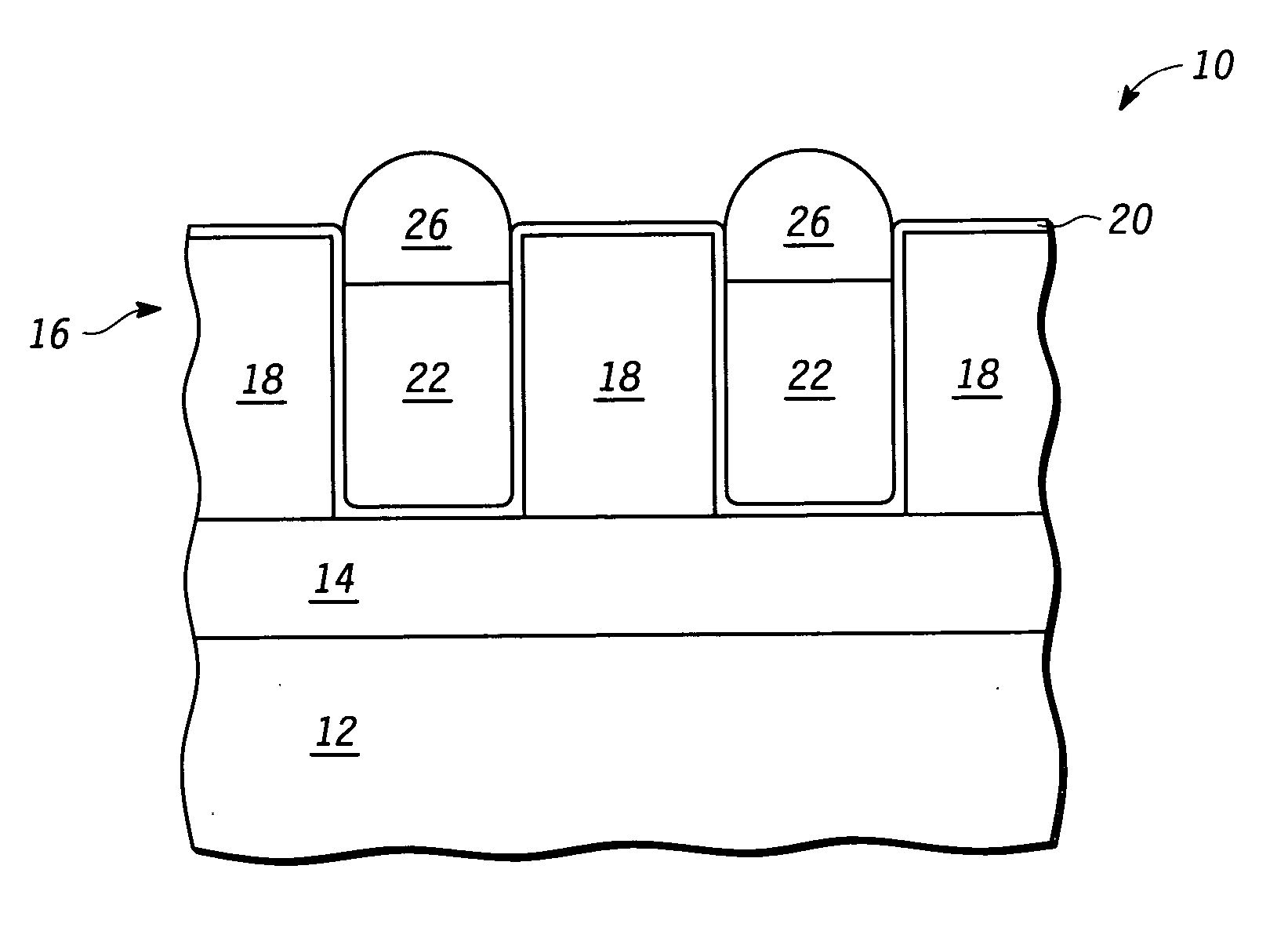
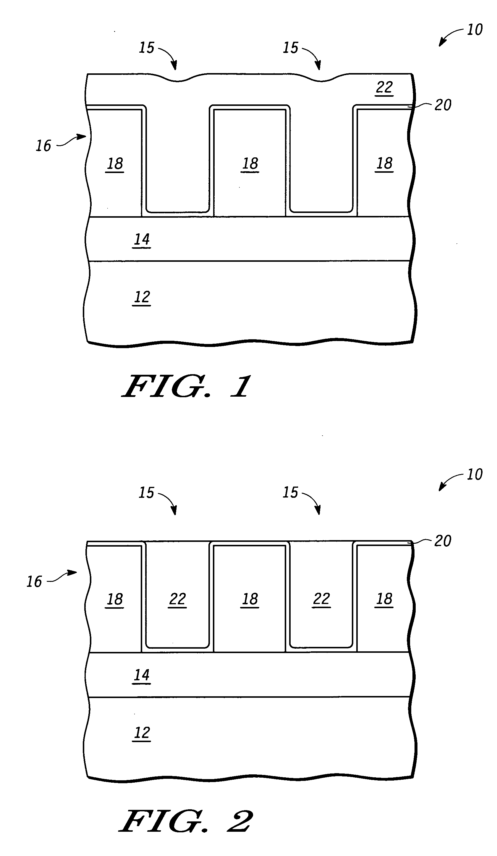
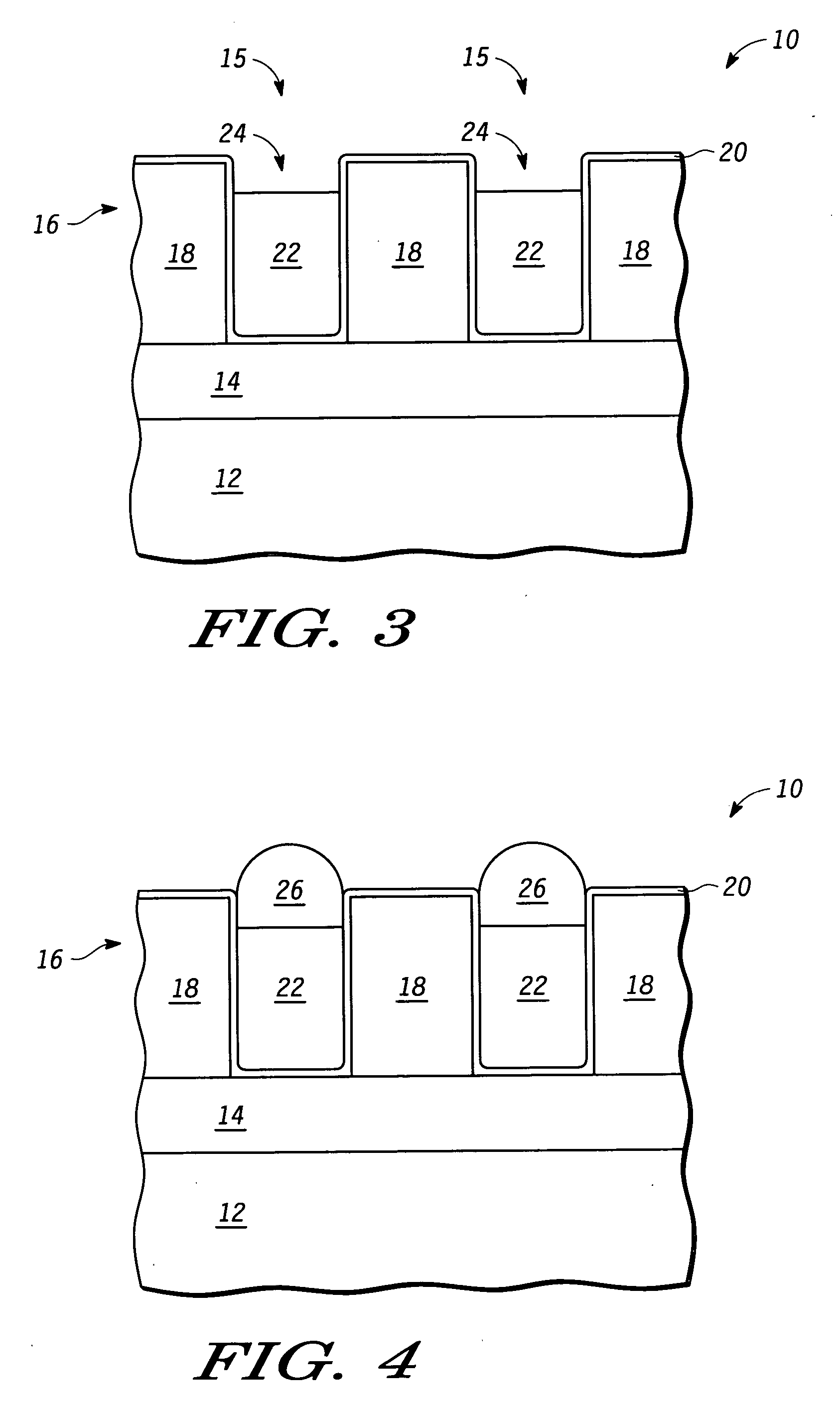
[0012] Generally, the present invention provides a method for forming a capping layer on top of a conductive metal layer that fills a cavity, such as a via or trench in an interconnect level of a semiconductor device. A purpose of the capping layer is to prevent diffusion of the conductive metal into subsequent interconnect levels within the device.

[0013] An active circuitry layer is formed on a substrate. The interconnect level is formed on top of the active circuitry level by depositing a dielectric layer and patterning the dielectric layer to form cavities, which can be vias, trenches, and the like. A diffusion barrier layer, such as tantalum or tantalum nitride, is deposited over the patterned dielectric layer such that the cavities and the top of the patterned dielectric layer are lined with the diffusion barrier layer. A conductive metal, such as copper, is deposited over the diffusion barrier layer, filling the cavities and forming a blanket film over the patterned dielectri...


PUM


Abstract

A method for making a semiconductor device includes forming a patterned dielectric overlying active circuitry, the patterned dielectric having a plurality of cavities. A diffusion barrier is formed over the patterned dielectric. A conductive layer is formed over the diffusion barrier in the plurality of cavities. The conductive layer is etched back to be below a top surface of the dielectric, forming recessed areas over the conductive layers in the plurality of cavities. The recessed areas are then filled with a capping film. The capping film and the diffusion barrier are removed to provide a relatively smooth planarized surface. Providing a relatively smooth planarized surface reduces leakage currents between conductors.

Description

RELATED APPLICATIONS [0001] A related, copending application is entitled “Method Of Forming A Semiconductor Device Having A Diffusion Barrier Stack And Structure Thereof”, by Michaelson et al., application Ser. No. 11 / 078,236, is assigned to the assignee hereof, and was filed Mar. 11, 2005.FIELD OF THE INVENTION [0002] The present invention relates generally to semiconductors, and more particularly, to a method for forming a capping layer on a semiconductor device. BACKGROUND OF THE INVENTION [0003] In integrated circuits, a dielectric layer is used to provide insulation around the interconnect wiring of the chip. Just as faster interconnect materials such as copper allow a signal to move faster through the chip, decreasing the capacitance factor of the insulating material also allows signals to travel across the interconnect faster because they have less interference with each other. The most common dielectric material is silicon dioxide. However, the semiconductor industry is cons...

Claims


Application Information

Patent Timeline
IPC IPC(8): H01L21/4763
CPCH01L21/76849H01L21/7684H01L21/28H01L21/4763
Inventor MARTIN, GERALD A.GARCIA, SAM S.MATHEW, VARUGHESE
Owner FREESCALE SEMICON INC
Features
  • R&D
  • Intellectual Property
  • Life Sciences
  • Materials
  • Tech Scout
  • Unparalleled Data Quality
  • Higher Quality Content
  • 60% Fewer Hallucinations
Learn More