Wiring board, process for producing the same polyimide film for use in the wiring board, and etchant for use in the process

a technology of polyimide film and wiring board, which is applied in the field of wiring board, can solve the problems of inability to form the fine via hole, the current mechanical drilling hits a technical limit, and the fabrication profile is more serious, and achieves the effect of efficient drilling

Inactive Publication Date: 2007-03-22
KANEKA CORP
View PDF4 Cites 23 Cited by
  • Summary
  • Abstract
  • Description
  • Claims
  • Application Information

AI Technical Summary

Benefits of technology

[0029] Through continuous effort to achieve these objectives, the inventors of the present invention have found out that the use of an etchant of a particular composition makes it possible to extremely efficiently form holes in a desired shape with no edge profile deformation through an organic insulating layer made of a polyimide, which has brought the present invention to completion.

Problems solved by technology

Therefore, in forming such fine holes, more serious problems arise in terms of fabrication profile.
First, current mechanical drilling hits a technical limit when used to form via holes measuring less than about 70 μm in diameter, being incapable of forming the aforementioned fine via holes.
In addition, if used to form 0.5 mm or smaller fine holes or slits, current mechanical drilling may develop burrs and irregular hole or slit edge profiles and cannot relied upon for high quality holes and slits.
Further, the technology requires a lot of labor in keeping a metal mold in good condition and presents obstacles in reducing costs.
Plasma dry etching is very poor in performance (processing speed), capable of forming only a limited number of holes per unit time.
However, etching a 20-μm-thick organic insulating layer using the technology takes as long as 80 minutes or so.
Processing with laser entails different problems in profile from mechanical drilling.
Less area will be available for wiring pattern on the surface of the organic insulating layer, which presents an obstacle in designing a high density wiring pattern.
Wet technology also has problems as follows, in forming fine holes:
These hydrazine-containing etchants (hydrazine etchants) have short a short lifespan (liquid life) during which the etchants remain efficacious; the short term validity makes it difficult to use them in etching in optimized conditions.
Besides, the etchants themselves are toxic (may cause cancer).
Accordingly, with the copper layer on the polyimide film being used as the mask, the etching with any of the etchants results in the copper layer peeling off the polyimide film before holes are formed through the polyimide film, and is likely to fail to form desired holes.
Those etchants are significantly inferior to the hydrazine etchants noted earlier in etching speed and likely to etch out deformed holes (having a profile and dimensions which do not conform to predefined conditions).
Further, if etching temperature is set to a higher value to speed up etching, the urea decomposes and produces ammonium which has irritating odor.
Results may be environmental health issues and grossly shortened liquid life, which render the use of the etchants hardly practical.
The etchant is made suitable for the purpose of dissolving commercially available, alkali-resistant photoresist materials (FSR-220, a product of Fuji Chemical Co. Ltd., is an example) and therefore readily infiltrate between polyimide and the alkali-resistant photoresist material, making it difficult to deliver a desired etching profile.
As detailed in the foregoing, both dry and wet technology has shortcomings and has issues waiting to be solved to apply to the multilayer printed wiring board.

Method used


Image

  • Wiring board, process for producing the same polyimide film for use in the wiring board, and etchant for use in the process
  • Wiring board, process for producing the same polyimide film for use in the wiring board, and etchant for use in the process
  • Wiring board, process for producing the same polyimide film for use in the wiring board, and etchant for use in the process

Examples


example 1

[0219] The polyimide film obtained by polyimide preparation method example 1 was attached onto a aluminum board using polyimide tape, so that it would constitute an organic insulating layer. Thereafter, a thin chromium film layer (first metal layer) and a thin copper film layer (second metal layer) were concurrently vapor deposited on the polyimide layer, using a sputtering device (sputtering system manufactured by Shimadzu Corporation; product name HSM-720). A metal layer which was made up of the chromium layer and the copper layer was thus formed on one surface of the aluminum board.

[0220] In the sputtering, argon as a sputtering ion source was introduced into a chamber. The chromium layer was vapor deposited at 1×10⁻² Torr, 0.2 A, for 90 seconds; the obtained chromium layer was about 500 Å thick. As the vapor deposition for copper, conditions were 5×10⁻³ Torr, 0.5 A, and 60 minutes; the obtained copper layer was about 7 μm thick.

[0221] Thereafter, the aluminum board was turned ...

example 3

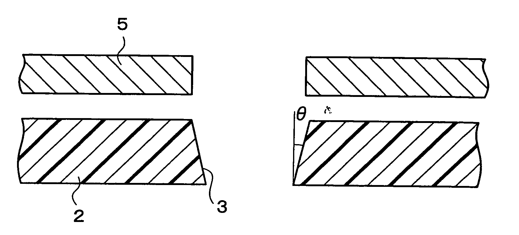
[0237] Wiring board (3) of the present invention was prepared in the same manner as in example 2 above, except that the polyimide film was subjected to atmospheric pressure plasma processing before stacked on a surface of the aluminum board. Wiring board (3) was inspected to measure the taper angle and the hole edge profile deformation and to count the number of holes having developed an edge profile deformation; results are listed in table 1 in columns (I), (III), and (IV) respectively.

example 4

[0239] Wiring board (4) of the present invention was prepared in the same manner as in example 3 above, except that the etchant used was a water solution prepared to provide a mixture ratio in weight, (potassium hydroxide) (water): (ethanol): (2-ethanolamine)=1:1.6:0.4:1. Wiring board (4) was inspected to measure the taper angle and the hole edge profile deformation and to count the number of holes having developed an edge profile deformation; results are listed in table 1 in columns (I), (III), and (IV) respectively.


PUM

PropertyMeasurementUnit
taper angleaaaaaaaaaa
diameteraaaaaaaaaa

Abstract

In etching an organic insulating layer made of a polyimide film, a polyimide containing at least a recurrent unit expressed by general formula (1) is used for the polyimide film:
;and an alkaline etchant containing oxyalkylamine, a hydroxide of an alkaline metal compound, water, and preferably an aliphatic alcohol is used as an etchant. The composition enables efficient formation of desirably shaped via holes and through holes through the organic insulating layer on a wiring board.

Description

FIELD OF THE INVENTION [0001] The present invention relates to wiring boards suitably used as components in various electronics and their methods of manufacture, as well as polyimide films suitably used on the wiring boards and etchants suitably used according to the methods of manufacture. BACKGROUND OF THE INVENTION [0002] Recent years have seen high demands in electronics industry for more capable, functional, and compact electronics. This trend is a cause for the on-going development of IC chip-carrying boards with more densely packed wiring. [0003] An electronic circuit board contains a copper layer (copper-based electric layer) as a typical metal layer and an organic insulating layer made of organic resin as an insulating layer. Conventionally, the organic insulating layer was a polyimide in order to exploit its excellent heat resistance and electrical properties. [0004] What counts in mounting components to these circuit boards, especially printed wiring boards (or printed ci...

Claims


Application Information

Patent Timeline
Patent Type & Authority Applications(United States)
IPC IPC(8): H01B13/00H05K1/00C08J7/12H05K1/03H05K3/00
CPCC08J7/12C08J2379/08H05K1/0346H05K2203/122H05K2201/0154H05K2203/0554H05K2203/0793H05K3/002C08G73/12
Inventor ONO, KAZUHIROFUJIHARA, KANAKAHORI, KIYOKAZU
Owner KANEKA CORP
Why Eureka
Try Eureka