Aluminum nitride thin film, composite film containing the same and piezoelectric thin film resonator using the same
a technology of aluminum nitride and composite film, which is applied in the field of piezoelectric thin film, can solve the problems that the piezoelectric thin film resonator or piezoelectric thin film filter that exhibits sufficient performance at a gigahertz band has not been achieved, and achieves excellent piezoelectric thin film, improve remarkably characteristics, and high crystallinity
- Summary
- Abstract
- Description
- Claims
- Application Information
AI Technical Summary
Benefits of technology
Problems solved by technology
Method used
Image
Examples
example 1
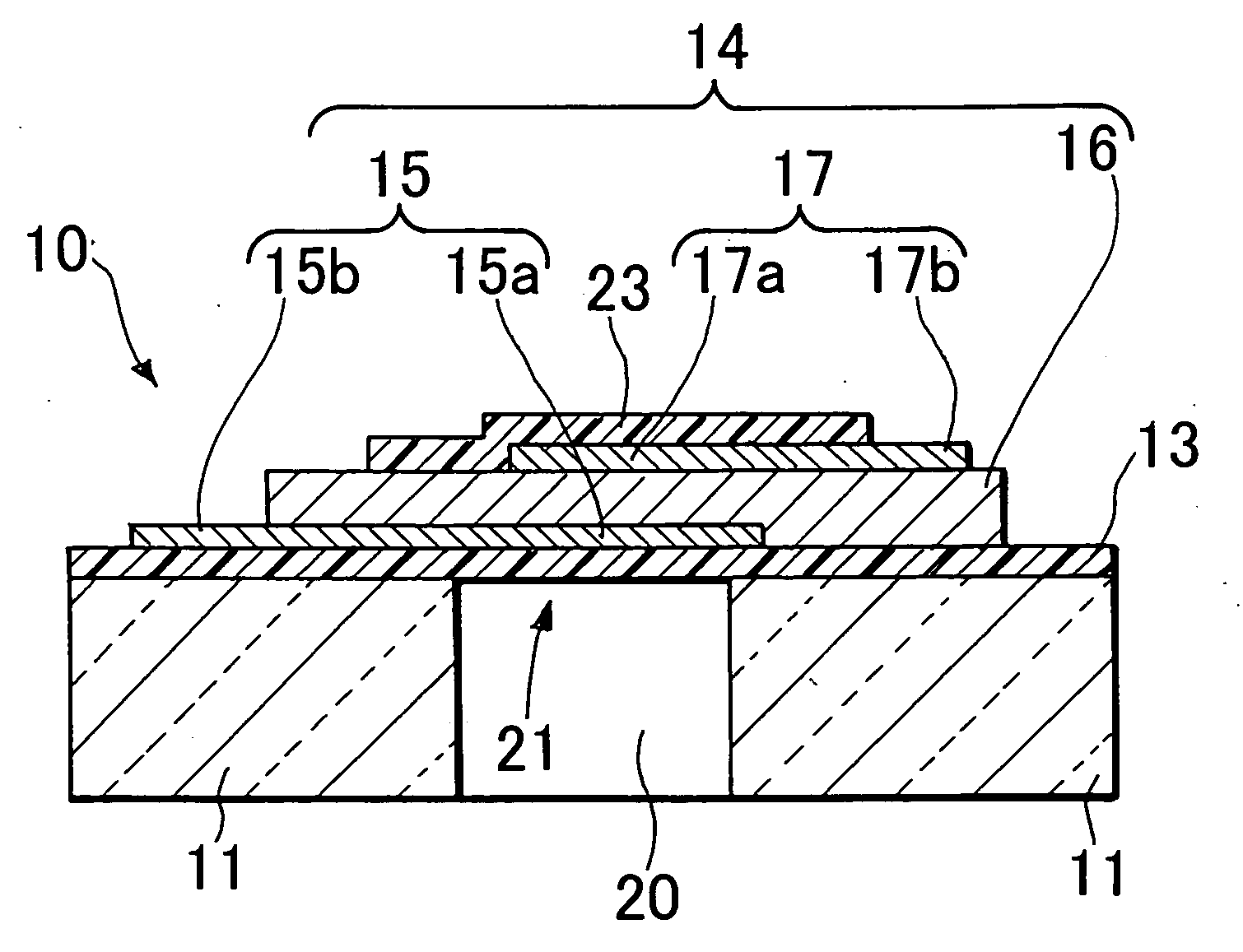
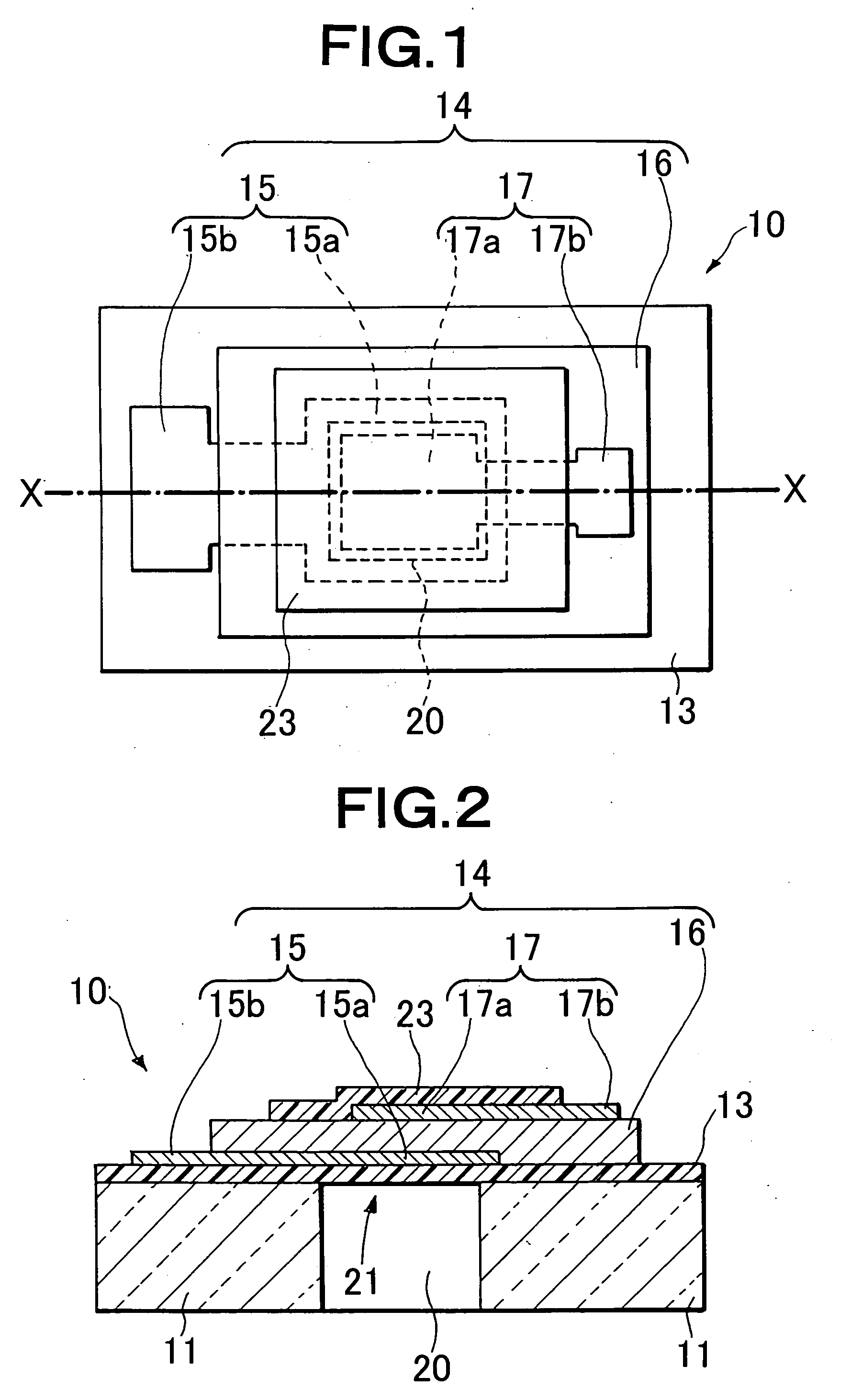
[0089] In this example, a piezoelectric thin film resonator having a structure shown in FIGS. 1 and 2 was manufactured as follows.
[0090] Specifically, an SiO2 layer having a thickness of 1,000 nm was formed by a thermal oxidation method on each of both surfaces of a (100) Si substrate having a thickness of 300 μm. Thereafter, a mask pattern corresponding to the shape of the via hole 20 was formed on a second surface (lower surface) side, and a part of the SiO2 layer which corresponds to the pattern was etched and removed. Simultaneously, all the SiO2 layer in a first surface (upper surface) side was etched and removed. Next, an Al2O3 thin film having a thickness of 220 nm was formed on the first surface side by a reactive sputtering method. On a first surface of this Si substrate, a Mo thin film having a thickness of 90 nm and an Ru thin film having a thickness of 100 nm were deposited orderly by a DC magnetron sputtering method, to form a lower electrode layer. Further, patterning...
example 2
[0092] In this example, a piezoelectric thin film resonator having the structure shown in FIGS. 1 and 2 was manufactured as follows. Specifically, the piezoelectric thin film resonator shown in FIGS. 1 and 2 was manufactured by similar methods to those in Example 1 except that the materials and thicknesses of the lower and upper insulating layers, the forming conditions and thickness of the Ru / Mo-layered lower electrode, and the material and thickness of the upper electrode were changed. Tables 1 and 2 show the material and thickness of each layer at the vibration portion, and a full-width half maximum (FWHM) of a rocking curve of the Ru / Mo-layered lower electrode. Table 3 shows a full-width half maximum (FWHM) of a rocking curve of the AlN thin film.
[0093] Further, a GSG micro prober manufactured by Cascade Microtech Inc. and a network analyzer were used to measure an impedance characteristic between the electrode terminals 15b and 17b of the piezoelectric thin film resonator. In ...
example 3
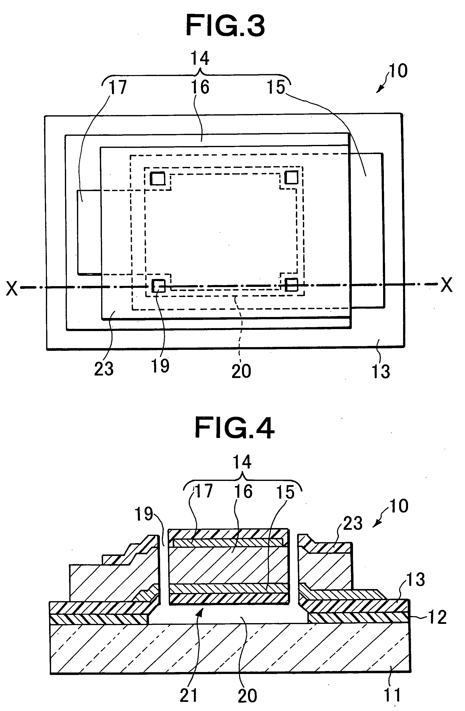
[0094] In this example, a piezoelectric thin film resonator having the structure shown in FIGS. 3 and 4 was manufactured as follows. Specifically, an SiO2 layer having a thickness of 1,500 nm was formed by a thermal oxidation method on each of both surfaces of an Si substrate having a thickness of 625 μm. Thereafter, a Ti thin film having a thickness of 50 nm to become a sacrifice layer was deposited on a first surface (upper surface) of the Si substrate, and a pattern was formed into a desired air bridge shape by photolithography. Next, an AlN thin film having a thickness of 100 nm was formed on the first surface side by a reactive sputtering method. On the first surface of this Si substrate, a Mo thin film and a Ru thin film which had thicknesses shown in Table 1 were deposited orderly by a DC magnetron sputtering method to form a lower electrode layer, which was further patterned by photolithography. In the pattern formation, resist was exposed to intentionally defocused ultravio...
PUM
 Abstract
Description
Claims
Application Information


