
Ferrite material and ceramic substrate

Inactive Publication Date: 2007-04-19
KYOCERA CORP
View PDF3 Cites 25 Cited by
  • Summary
  • Abstract
  • Description
  • Claims
  • Application Information

AI Technical Summary

Benefits of technology

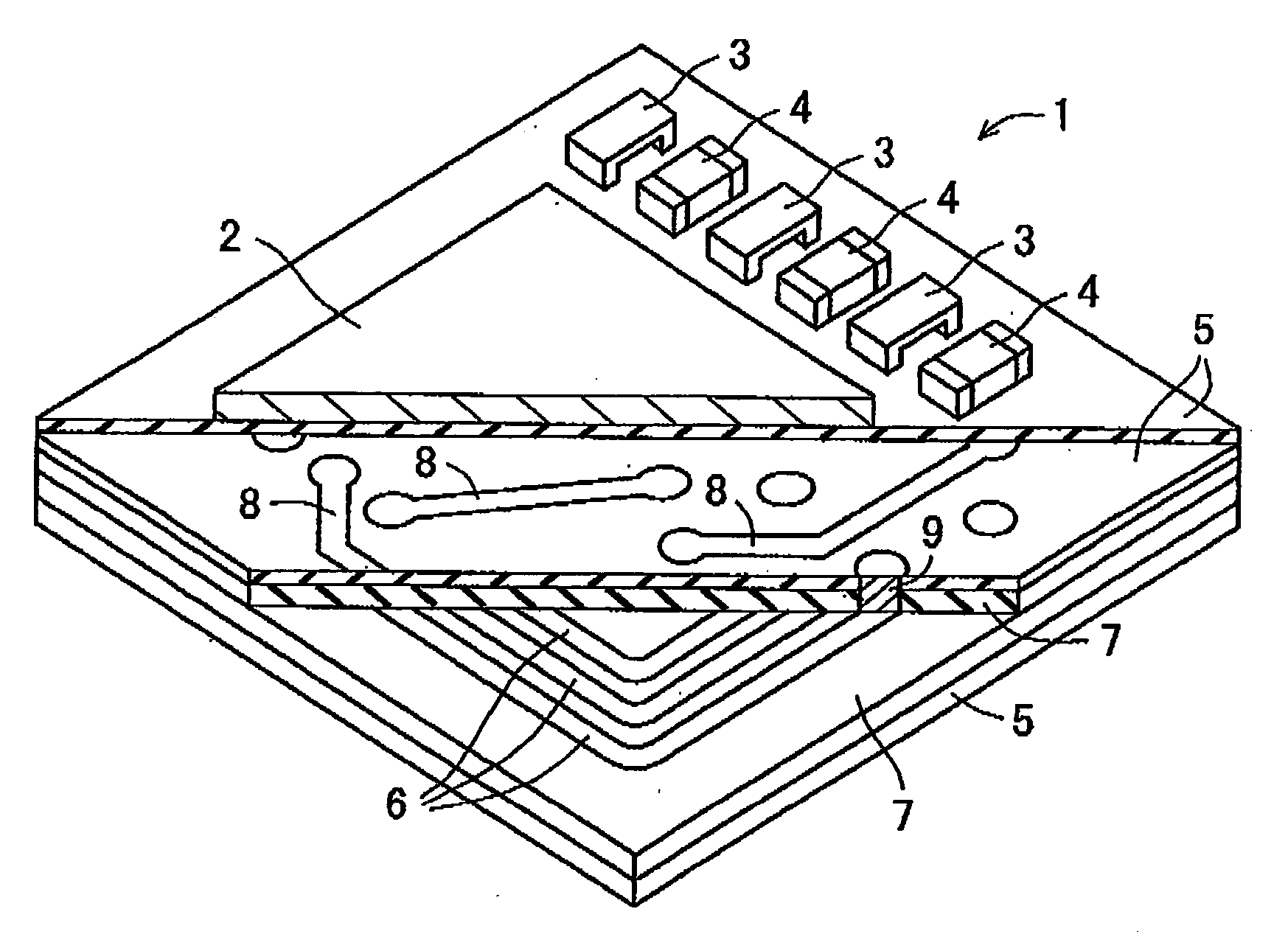
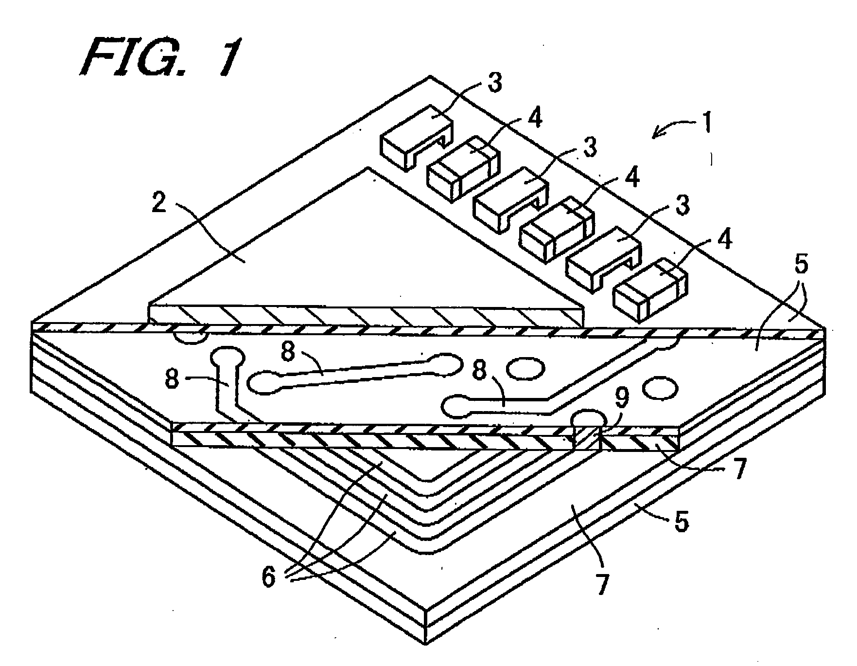
[0021] Another object of the invention is to provide a glass ceramic substrate having a ferrite layer made of the above-described low-temperature firable, high-magnetic permeability ferrite material in which is embedded a coil-shaped conductor layer that exhibits a high inductance with stability.
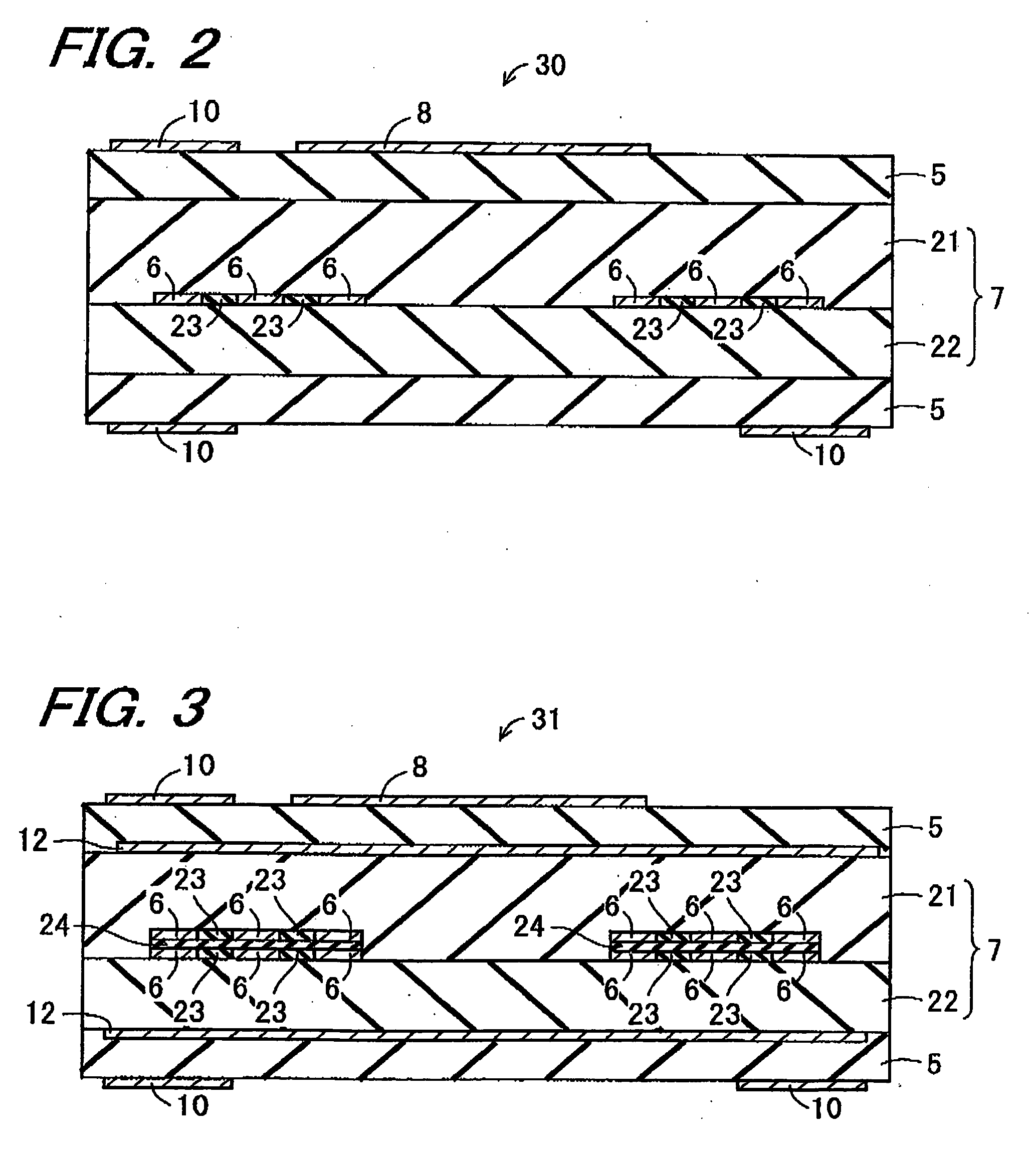
[0057] According to the ceramic substrate of the invention, the glass ceramic insulating layer and the ferrite layer are bonded to each other via the intermediary layer formed of a sintered metal layer composed of glass and at least one kind of metal selected from among Cu, Ag, Au, Pt, Ag—Pd alloy, and Ag—Pt alloy. In this case, a stress resulting from the difference in thermal expansion coefficient between the ferrite layer and the glass ceramic insulating layer can be alleviated by plastic deformation of the sintered metal layer. As a result, an undesirable decrease in magnetic permeability caused by magnetic distortion can be suppressed, and also the ferrite layer and the glass ceramic insulating layer can be bonded to each other more securely.

Problems solved by technology

Therefore, inclusion of such a coil as allows acquisition of a relatively high inductance of approximately 100 nH cannot be achieved without increasing the number of turns in the coil.
This gives rise to the impossibility of achieving compactness and slimness for the substrate in an effective manner.
However, a glass ceramic substrate having a ferrite layer of conventional design has encountered the following problems.
The first problem is the low magnetic permeability of the ferrite layer interposed between the glass ceramic layers.
As a consequence, the ferrite density in the ferrite layer is decreased and this leads to poor magnetic permeability.
Furthermore, in the case of firing the ferrite layer and the glass ceramic insulating layer at one time, because of the significant difference in thermal expansion coefficient between the ferrite layer and the glass ceramic insulating layer, the ferrite layer is subjected to a stress in the course of firing, in consequence whereof there results magnetic distortion.
This leads to an undesirable decrease in the magnetic permeability of the ferrite layer.
The second problem is spalling of the ferrite layer.
That is, when the ferrite layer is increased in thickness to obtain a sufficiently high inductance, due to the stress resulting from the difference in thermal expansion coefficient between the ferrite layer and the glass ceramic substrate, the ferrite layer is prone to come off after the completion of firing.
The third problem is roughening of the glass ceramic substrate due to inadequate sintering.
As a consequence, the ferrite layer lying in the inside of the glass ceramic substrate cannot be sintered properly, thus causing undesired roughening.
If, for example, atmospheric moisture finds its way into the exposed part, the glass ceramic substrate becomes water-absorptive, which leads to deterioration of the electrical characteristics of the glass ceramic substrate, such as occurrence of a short circuit in the wiring conductor disposed in the inner layer of the glass ceramic substrate.
After all, the glass ceramic substrate offers poor electrical reliability.
In a case where a wiring is disposed directly on the surface of the ferrite layer, a high inductance is induced in the wiring, thus causing noise.
This may possibly give rise to a circuitry malfunction.
However, the use of non-magnetic ferrite poses the following problems.
Because of the instability of the magnetic lines of force, the ferrite layer is liable to undergo magnetic saturation caused by a disturbance of the magnetic lines of force.
Thus, upon application of a large current, there occurs a decrease in inductance; that is, the so-called superposition characteristics are impaired.
Furthermore, the magnetic lines of force radiating toward the exterior of the ceramic substrate are liable to have an electrical influence on the semiconductor chip, chip component, and wiring mounted on the upper and lower surfaces of the ceramic substrate, thus causing a circuitry malfunction.
As a result, the ceramic substrate is increased in thickness as a whole, thus making it impossible to realize a slimmed-down substrate.
Secondly, in the conventional ceramic substrate constructed by forming a ferrite layer and a coil-shaped conductor layer inside a non-magnetic ferrite substrate, in a case where metallized wiring layers are formed on the surface or in the inside of the substrate, if the thickness of the non-magnetic ferrite layer constituting the insulator substrate is reduced to make the substrate smaller in size and lower in profile, a leakage current will occur between the metallized wiring layers.

Method used


Image

  • Ferrite material and ceramic substrate
  • Ferrite material and ceramic substrate
  • Ferrite material and ceramic substrate

Examples


example 1

[0135] Raw materials of varying composition as given in Table 1 were adjusted to weigh 250 g on an individual basis. The constituents of the raw material have been blended with a liter of pure water for 24 hours in a 2-liter ball mill constructed of a zirconia pulverization ball. Following a fractional drying process, the raw material powder was fired tentatively in a zirconia crucible at a temperature of 730° C. After it has been determined that there is obtained a desired compound by means of X-ray diffraction, the raw material was pulverized into small particles by a ball mill and dried. The powder particles were sifted out through a mesh sieve to obtain tentatively-fired powder having a particle size of 0.5 to 0.7 μm. Subsequently, the powder was granulated by a stone mill, with a 10% by mass of PVA solution added. The granulated powder thus obtained was subjected to stamping with a die and fired in an air atmosphere at a temperature of 900° C. for two hours. In so doing there w...

example 2

[0141] To begin with, a non-magnetic ferrite green sheet was formed as follows to form a non-magnetic ferrite layer acting as an insulating layer. At first 630 parts by mass of Fe2O3 powder, 80 parts by mass of CuO powder, and 290 parts by mass of ZnO powder are blended with 4000 cm3 of pure water for 24 hours in a 7000 cm3-ball mill constructed of a zirconia pulverization ball. Following a fractional drying process, the raw material powder is fired tentatively in a zirconia crucible at a temperature of 730° C. In do doing there is prepared tentatively-fired non-magnetic ferrite powder. Subsequently, 10% by mass of butyral resin and, as a diluent, 45% by mass of alcohol of high molecular weight are added with respect to 100% by mass of the tentatively-fired non-magnetic ferrite powder thus obtained. They are blended together by a ball mill technique to form a slurry. The slurry is then formed into a 100 μm-thick non-magnetic ferrite green sheet by the doctor blade method.

[0142] The...

example 3

[0152] A ceramic substrate was fabricated by way of Example 3 basically in the same manner as in Example 2, the only difference being that electromagnetic shielding layers are interposed between the first ferrite layer and one insulating layer and between the second ferrite layer and the other insulating layer, respectively, face to face with the planar spiral coil. The electromagnetic shielding layers were formed as follows. At first 12 parts by mass of acrylic resin and 2 parts by mass of α-terpineol acting as an organic solvent are added with respect to 100 parts by mass of Ag powder. They are blended thoroughly by an agitating / defoaming machine and then kneaded thoroughly by a three-roll mill to form a conductor paste. The conductor paste is applied to the predetermined regions in a thickness of 20 μm by the screen printing technique, the area of which is one-half that of the planar spiral coil. Lastly, the coating is dried for 30 minutes at a temperature of 70° C. Measurement w...


PUM

PropertyMeasurementUnit
Percent by massaaaaaaaaaa
Electrical resistanceaaaaaaaaaa

Abstract

A low-temperature firable ceramic substrate having formed in its inside a ferrite layer with a coil embedded therein is provided. The ferrite layer has a composition of 63 to 73% by mass of Fe2O3, 5 to 10% by mass of CuO, 5 to 12% by mass of NiO, and 10 to 23% by mass of ZnO. Even if firing is performed at a lower temperature than ever, it is possible to obtain a ferrite layer which is excellent in sintered density and magnetic permeability.

Description

BACKGROUND OF THE INVENTION [0001] 1. Field of the Invention [0002] The present invention relates to a ferrite material and a LTCC (Low Temperature Cofire Ceramic) substrate having formed in its inside a ferrite layer made of the ferrite material in which is embedded a coil-shaped conductor layer. [0003] 2. Description of the Related Art [0004] To date electronic equipment such as a mobile communication apparatus, typified by a cellular telephone, has been designed to have a multiplicity of electronic devices incorporated therein. In recent years, communication apparatuses such as a cellular telephone have been becoming smaller in size so rapidly that downsizing and slimming have been sought after in various electronic devices designed to be mounted therein. For example, there is known an LC filter constructed by disposing a coil within a glass ceramic substrate. In the LC filter, in contrast to a conventional LC filter to which a coil, or a chip component is added externally, a coi...

Claims


Application Information

Patent Timeline
IPC IPC(8): H01L29/94
CPCB32B18/00C04B35/265H01L2924/0002C04B35/6261C04B2235/3279C04B2235/3281C04B2235/3284C04B2235/36C04B2235/5445C04B2235/6025C04B2235/77H01F10/20H01F17/0006H01F41/046H01F2017/008H01L23/13H01L23/15H01L23/49822H01L23/552H01L23/645H01L2924/09701H01L2924/19105H01L2924/3011H05K1/0306H05K1/165H05K3/4626H05K3/4629H05K3/4688H05K2201/0187H05K2201/086H01F10/265H01L2924/00
Inventor MIKURA, TSUTOMUIKEDA, KOTANAKAHARA, KOICHI
Owner KYOCERA CORP
Learn More