Electric appliance, semiconductor device, and method for manufacturing the same

a technology of semiconductor devices and electric appliances, applied in the field of semiconductor devices, can solve the problems of high cost, large loss of material solution or waste liquid, and the film formation method of using spin coating becomes at a disadvantage in mass production, so as to reduce the amount of material and reduce the cost. cost

Inactive Publication Date: 2007-04-26
SEMICON ENERGY LAB CO LTD
View PDF10 Cites 59 Cited by
  • Summary
  • Abstract
  • Description
  • Claims
  • Application Information

AI Technical Summary

Benefits of technology

[0046] A microscopic wiring pattern can be obtained by droplet discharging according to the present invention. The present invention can reduce drastically costs since a patterning process can be shortened and an amount of material can be reduced. Accordingly, the present invention can be applied to manufacture a large substrate.

Problems solved by technology

When the substrate size is further increased in a future, the film formation method of using spin coating becomes at a disadvantage in mass production since a rotation mechanism for rotating a large substrate becomes large and there is much loss of material solution or waste liquid.

Method used


Image

  • Electric appliance, semiconductor device, and method for manufacturing the same
  • Electric appliance, semiconductor device, and method for manufacturing the same
  • Electric appliance, semiconductor device, and method for manufacturing the same

Examples


embodiment 1

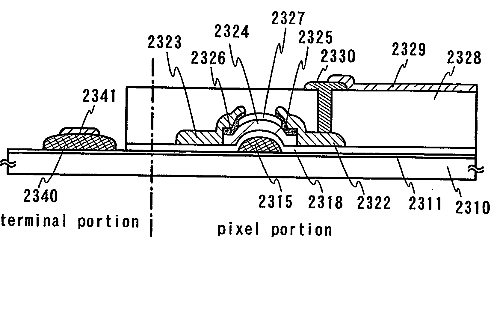
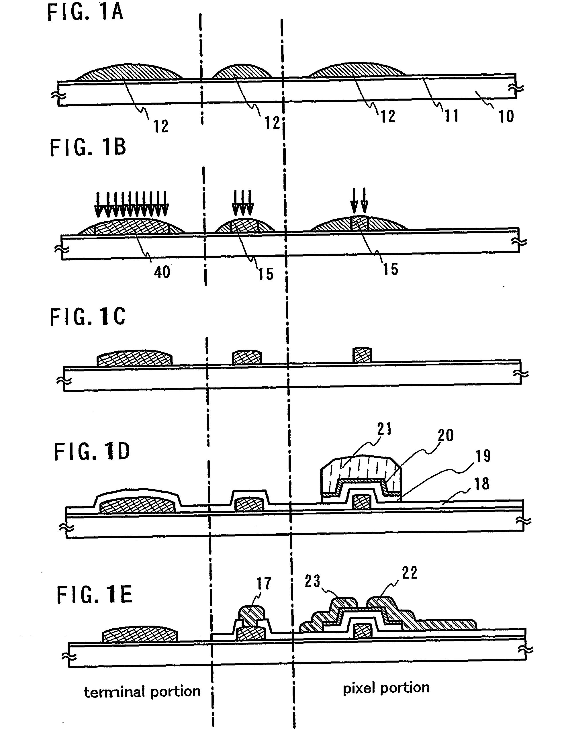
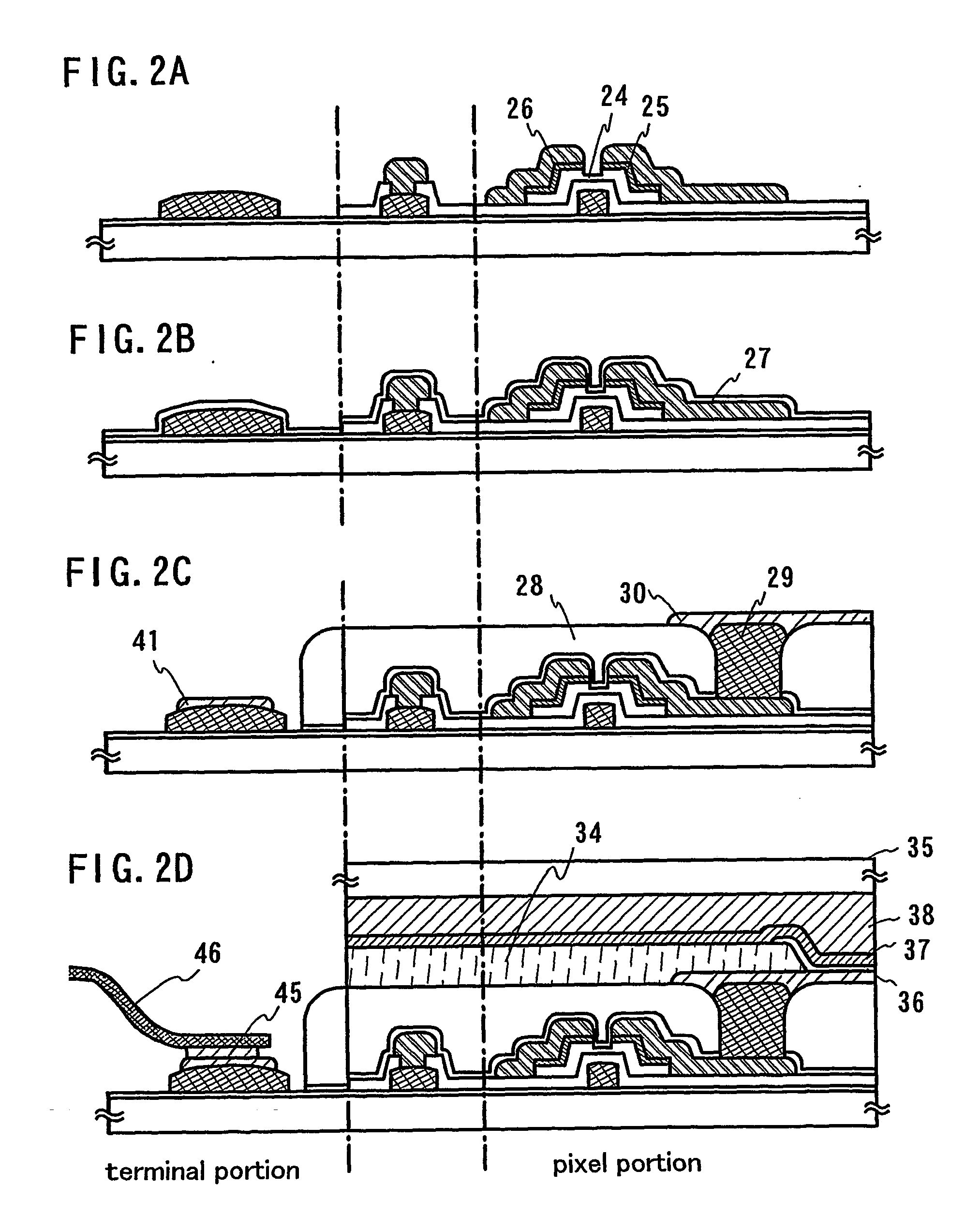
[0081]FIGS. 1A to 2D illustrate a method for manufacturing an active matrix light-emitting display device having a channel etch type TFT as a switching element.

[0082] A base layer 11 for improving adhesiveness between a substrate 10 and a material layer that is formed later by droplet discharging is formed over the substrate 10. Since the base layer 11 may be formed to have an ultra thin thickness, the base layer is not always required to have a layered structure. The form of the base layer 11 can be considered as base pretreatment. Treatment such that a photocatalyst material (titanium oxide (TiOx), strontium titanate (SrTiO3), cadmium selenide (CdSe), potassium tantalate (KtaO3), cadmium sulfide (CdS), zirconium oxide (ZrO2), niobium oxide (Nb2O5), zinc oxide (ZnO), iron oxide (Fe2O3), tungsten oxide (WO3)) is dropped over the whole surface by spraying or sputtering may be performed. Alternatively, treatment such that an organic material (polyimide, acrylic, or a coated insulatin...

embodiment 2

[0157] Embodiment 1 explains an example of exposing a gate wiring by a laser beam drawing device. Here, an example of a process that uses a laser beam drawing device for forming a source wiring or a gate wiring with reference to FIG. 5.

[0158] The process differs slightly from that explained in Embodiment 1, and so the same part of the process is not further explained for simplification.

[0159] Similar to Embodiment 1, up to a patterning process of a semiconductor film is performed. Then, a conductive film pattern 220 is formed by droplet discharging (FIG. 5A). A positive type photosensitive material is mixed into the conductive film pattern 220.

[0160] Then, the conductive film pattern 220 is selectively exposed to laser light by using the device illustrated in FIG. 4 (FIG. 5B). A portion 221 that is irradiated with the laser light brings about chemical reactions.

[0161] The portion 221 that is irradiated with laser light by developing is removed to form a source wiring or a drain ...

embodiment 3

[0166]FIGS. 6A to 6D illustrate examples of other processes. In FIGS. 6A to 6D, an example of using a planarizing film as a gate insulating film 260. Other components are the same as those explained in Embodiment 2.

[0167] After forming a gate electrode, the gate insulating film 260 having a plane surface is formed by sputtering, a planarizing treatment of a film obtained by chemical vapor deposition, or coating method. The planarizing treatment is typified by chemical mechanical polishing treatment.

[0168] In the case of manufacturing a light-emitting display device having a large screen, a gate wiring having low resistance may be preferably formed to have a thick thickness, for example, of 1 to 5 μm. When a cross-sectional area is increased by increasing the thickness of a wiring, difference in level between the surface of the substrate and the surface of the thick film wiring is produced, which leads to deterioration of coverage. The plane gate insulating film 260 is useful in ca...


PUM

PropertyMeasurementUnit
sizeaaaaaaaaaa
sizeaaaaaaaaaa
sizeaaaaaaaaaa

Abstract

In the present circumstances, a film formation method of using spin coating in a manufacturing process is heavily used. As increasing the substrate size in future, the film formation method of using spin coating becomes at a disadvantage in mass production since a mechanism for rotating a large substrate becomes large, and there is many loss of material solution or waste liquid. According to the present invention, in a manufacturing process of a semiconductor device, a microscopic wiring pattern can be realized by delivering selectively photosensitive conductive material solution by droplet discharging, exposing selectively to laser light or the like, and developing. The present invention can reduce drastically costs since a patterning process can be shortened and an amount of material in a process of forming a conductive pattern can be reduced. Accordingly, the present invention can be applied to manufacture a large substrate.

Description

TECHNICAL FIELD [0001] The present invention relates to a semiconductor device and a method for manufacturing the semiconductor device having a circuit composed of thin film transistors (hereinafter, TFT). More specifically, the present invention relates to an electric appliance installed with an electro-optic device as typified by a light-emitting display device having an organic light-emitting element, or a liquid crystal display panel. [0002] As used herein, the term “semiconductor device” refers to a device in general that can operate by utilizing semiconductor characteristics such as an electro-optic device, a semiconductor circuit, and an electric appliance. BACKGROUND ART [0003] In recent years, technique of composing thin film transistors (TFT) by using a semiconductor thin film (with a thickness of approximately several to several hundreds nm) formed over a substrate having an insulating surface has attracted attention. A thin film transistor is widely applied to an electro...

Claims


Application Information

Patent Timeline
Patent Type & Authority Applications(United States)
IPC IPC(8): H01L21/84H01L21/00G02F1/1343G02F1/1362G02F1/1368G09F9/00H01L21/28H01L21/288H01L21/3205H01L21/336H01L21/768H01L21/77H01L29/417H01L29/423H01L29/49H01L29/786H05B33/14
CPCG02F2001/136295H01L21/288H01L21/76838H01L27/1292H01L29/41733H01L29/42384H01L29/4908H01L27/12G02F1/136295
Inventor MAEKAWA, SHINJIYAMAZAKI, SHUNPEISHOJI, HIRONOBU
Owner SEMICON ENERGY LAB CO LTD
Why Eureka
Try Eureka