

Method for plating printed circuit board and printed circuit board manufactured therefrom
Inactive Publication Date: 2007-05-10
SAMSUNG ELECTRO MECHANICS CO LTD +1
View PDF9 Cites 44 Cited by
- Summary
- Abstract
- Description
- Claims
- Application Information
AI Technical Summary
Benefits of technology
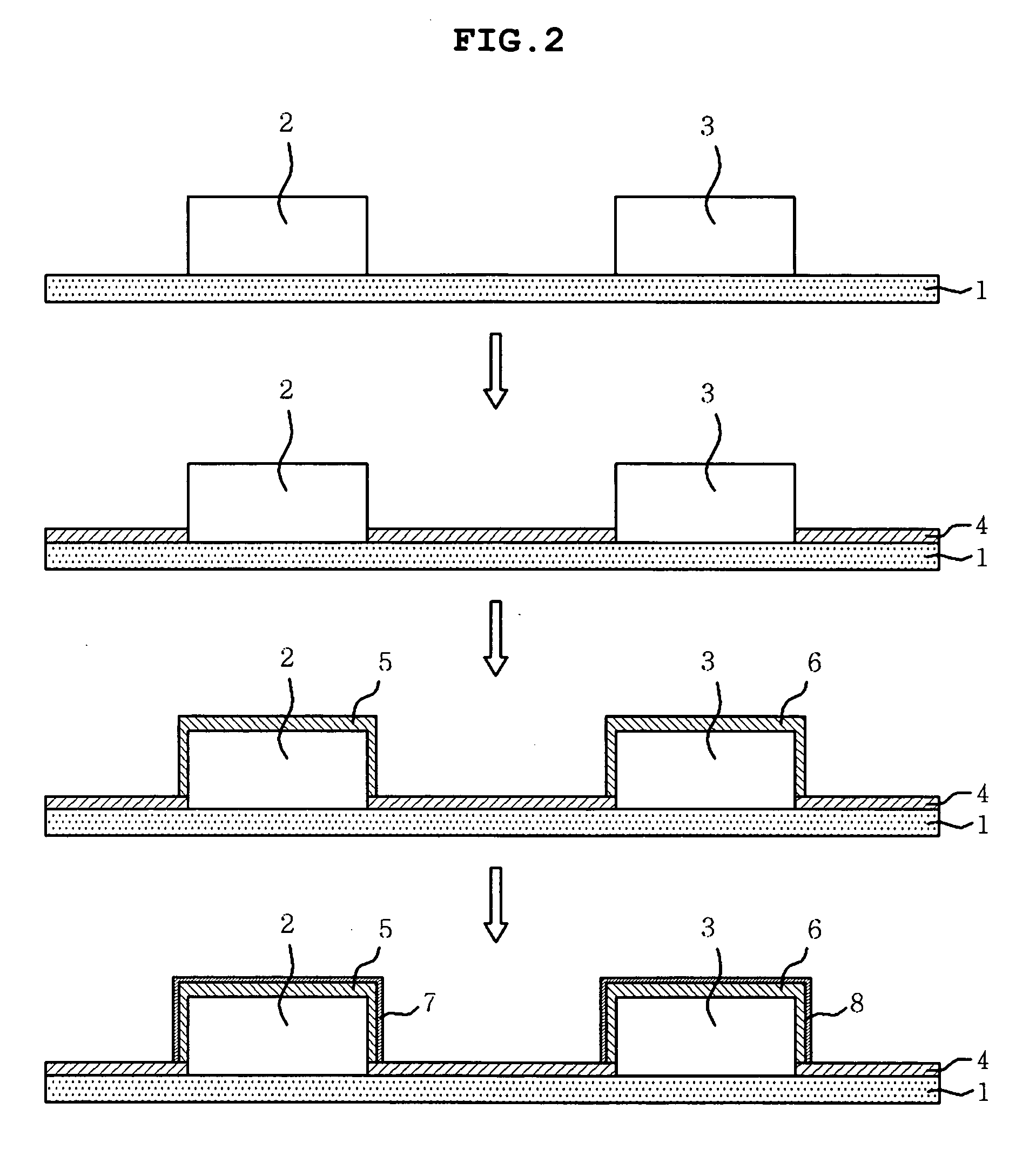
[0016] Leading to the present invention, intensive and thorough research, conducted by the present inventors aiming to solve the problems encountered in the prior art, into the formation of metal plated layer on PCBs, resulted in the finding that the intercalation of a palladium or palladium alloy plated layer between a copper layer and a gold plated layer can significantly reduce the thickness of the gold plated layer without decreasing wire bondability or solderability.
[0018] It is another object of the present invention to provide a method for plating a printed circuit board, which can significantly reduce production costs and greatly increase productivity without the occurrence of conventional technical problems including bending cracks, and a printed circuit board fabricated therefrom.
Problems solved by technology
If they remain bare or are externally exposed, the copper layers are likely to lose soldering or wire bonding properties as they oxidize or corrode over time.
When thin gold plating (flash gold plating, usually less than 0.1 μm) is conducted after nickel or nickel alloy plating, poor wire bondability results.
Also functioning as an antenna, the lead wire may cause a noise phenomenon after semiconductor assembly.
However, such removal is difficult to conduct perfectly.
Further, the plating solutions have much short lives, giving rise to an increase in production cost.
Rigid-flexible or flexible printed circuit boards, which have come into great demand with the miniaturization and multi-functionalization of portable electronic devices, are subjected to severe process conditions, such as bending and distortion, before being sold.
When subjected to such severe process conditions, printed circuit boards having electroless nickel plated and immersion gold plated layers exhibit problems fatal to their usefulness, since bending cracks are caused due to the high inherent strength of the nickel-phosphorus alloy and the structural transformation of the alloy according to thermal treatment.
Therefore, the PCBs with nickel plated thereon are not suitable for use in low current, high frequency applications.
Method used
View moreImage
Smart ImageViewing Examples

Examples
example 1
[0077] On the copper layer of the pre-treated printed circuit board, a palladium-phosphorus alloy comprised of a ratio of palladium:phosphorus 96.7:3.3 (wt %) was plated to a thickness of 0.2 μm, followed by the formation of a gold plated layer 0.05 μm thick on the palladium phosphorus alloy plated layer.
example 2
[0078] The same procedure as in Example 1 was repeated, with the exception that palladium-boron alloy comprised of a ratio of palladium:boron 99.3:0.7(wt %) was used instead of palladium-phosphorus.
example 3
[0079] The same procedure as in Example 1 was repeated, with the exception that pure palladium was used instead of the palladium alloy.
Login to View More PUM
| Property | Measurement | Unit |
|---|---|---|
| Temperature | aaaaa | aaaaa |
| Temperature | aaaaa | aaaaa |
| Time | aaaaa | aaaaa |
Abstract
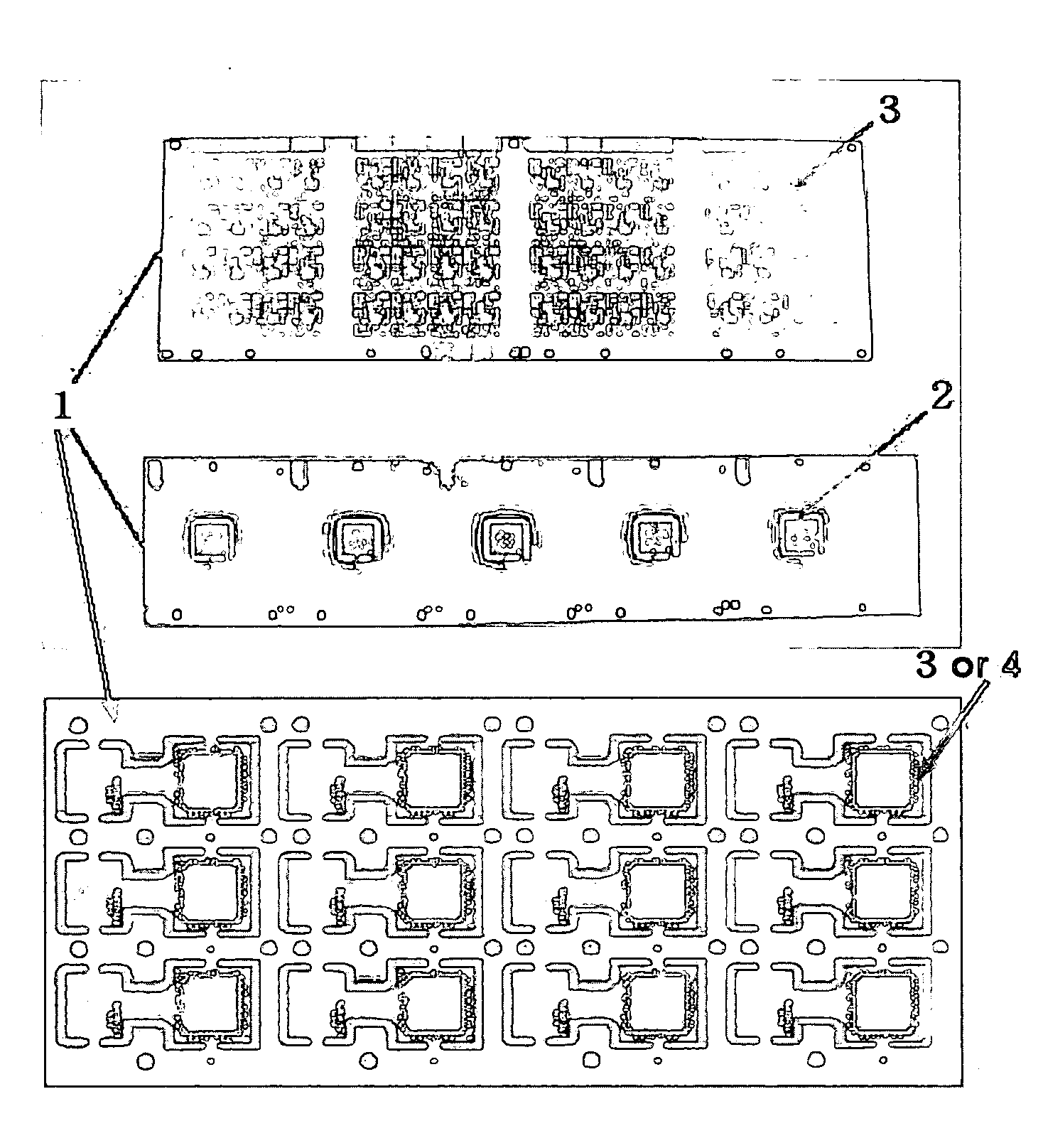
Disclosed herein are a method for plating a printed circuit board and the printed circuit board manufactured therefrom. In the method, a bare soldering or wire bonding portion of a copper (Cu)- or copper alloy layer, is plated with palladium (Pd) or a palladium alloy, and then gold (Au) or a gold alloy is deposited over the palladium or palladium alloy plated layer by an electroless substitution plating process based on ionization tendency. Having superior hardness, ductility and corrosion resistance, palladium is suitable for use between a connector and a substrate and meets requirements for the printed circuit board even when applied to a low thickness, greatly reducing the process time. Accordingly, the problem of black pad, which frequently occur on electroless nickel and electroless gold finish upon surface mount technology, can be perfectly solved. Particularly, fatal bending cracks can be prevented from occurring in the rigid-flexible or flexible printed circuit boards.
Description
CROSS REFERENCE TO RELATED APPLICATION(S) [0001] This application claims the benefit of Korean Patent Application No. 10-2005-0100787, entitled “Method for plating on printed circuit board and printed circuit board produced therefrom”, filed Oct. 25, 2005, which is hereby incorporated by reference in its entirety into this application. BACKGROUND OF THE INVENTION [0002] 1. Field of the Invention [0003] The present invention relates, in general, to a method for plating a printed circuit board and printed circuit board manufactured therefrom and, more particularly, to a method for plating a printed circuit board and printed circuit board manufactured therefrom, wherein said method comprises forming a palladium or palladium alloy plated layer on a bare copper in the printed circuit board by electroless substitution plating and forming a gold or gold alloy plated layer on the palladium or palladium alloy plated layer by electroless substitution plating. The instant printed circuit board...
Claims
Login to View More Application Information
Patent Timeline
 IPC IPC(8): B05D5/12B32B3/00
CPCH05K3/244H05K3/28H05K2203/072H05K2203/073C23C18/44Y10T428/24917H01L21/4846H01L23/498H01L2924/0002C23C18/54H01L2924/00H01L24/85H01L2224/45124H01L2224/85444H01L2224/45144H01L2924/00011H01L2924/01033H05K3/18
InventorYIM, KYU HYOKCHUN, SUNG WOOKYANG, DEK GINAN, DONG GILEE, CHUL MINHAN, MI JUNG
OwnerSAMSUNG ELECTRO MECHANICS CO LTD