Opc trimming for performance

a technology of opc and performance, applied in the field of semiconductor wafer processing, can solve the problems of inability to meet the needs of overexposure or reactive ion etch gate trimming, inability to reduce the amount of steps, and increase the current of off-state. the effect of performance and timing

Inactive Publication Date: 2007-05-10
GLOBALFOUNDRIES INC
View PDF12 Cites 16 Cited by
  • Summary
  • Abstract
  • Description
  • Claims
  • Application Information

AI Technical Summary

Benefits of technology

[0010] Bearing in mind the problems and deficiencies of the prior art, it is therefore an object of the present invention to provide a methodology for improving integrated circuit yield, performance, and timing.
[0011] It is another object of the present invention to provide an analytical method for improving the switching time of integrated circuit chip design.
[0012] A further object of the invention is to provide a higher performance and faster integrated circuit chip speed using gates that are generally given a higher lithographic dose and having a shorter gate length in terms of power flow.
[0013] It is yet another object of the present invention to provide a method for printing only selective circuits short in an integrated circuit chip, so that standby currents remain at an acceptable level.
[0015] The above and other objects, which will be apparent to those skilled in the art, are achieved in the present invention, which is directed to a method for optimizing an integrated circuit chip comprising: identifying timing sensitive devices that are within the critical timing path of the integrated circuit chip; and generating a mask to shorten gate lengths of each of the timing sensitive devices without shortening the gate lengths of devices that are not within the critical timing path. The method includes using optical proximity correction (OPC) techniques to generate the mask. A PT mask is analytically designed to shorten each of the gate lengths of the timing sensitive circuits only, without shortening the gate lengths of devices that are not within the critical timing path. Additionally, time sensitive devices may be analytically determined in the integrated circuit chip; marker shapes analytically applied to identify and locate the timing sensitive devices; and assigned shortened gate lengths applied to each of the timing sensitive devices. The method may also include the steps of generating a set of timing rules for the integrated circuit chip including the timing sensitive devices; comparing the set of timing rules to predetermined product requirements; shortening each of the gate lengths of the timing sensitive devices an incremental amount if the product requirements are not met by the set timing rules; and repeating the steps of comparing timing rules to product requirements and shortening the gate lengths until the product requirements are met. Furthermore, optimization data including gate lengths of the timing sensitive devices may be obtained when the product requirements are met; and a mask generated from the optimization data. The set of timing rules may then be compared to manufacturing limits and the mask may be generated from data less optimized than the optimization data when the manufacturing limits are reached or exceeded prior to obtaining design optimization. The step of generating the mask to shorten the gate lengths of each of the timing sensitive devices may include lowering threshold voltages for each of the timing sensitive devices.

Problems solved by technology

Overexposure or reactive ion etch trim of gates cannot address the need for strengthening individual devices or subgroups since the entire chip or wafer is affected by these processes.
Strengthening the devices by lowering the threshold voltage is typically considered a granular remedy resulting in a threshold voltage step function with steps that are often too few and too large.
Moreover, in most instances, the remedy of lowering the threshold voltages may have already been chosen, thus representing an exhausted option.
Additionally, lowered threshold voltages will cause the off-state leakage current to increase dramatically.
Adding an additional mask for a selective polysilicon trim (PT) would allow for only one step, and would not allow for fine tuning the design.
These effects may lead to an operating situation where the chip exceeds its thermal cooling capacity.
These devices have a standby current that is unacceptably high, and may represent a majority of the yield.
The higher the standby current, the more likely the devices will exceed their thermal cooling capacity.

Method used


Image

  • Opc trimming for performance
  • Opc trimming for performance
  • Opc trimming for performance

Examples


first embodiment

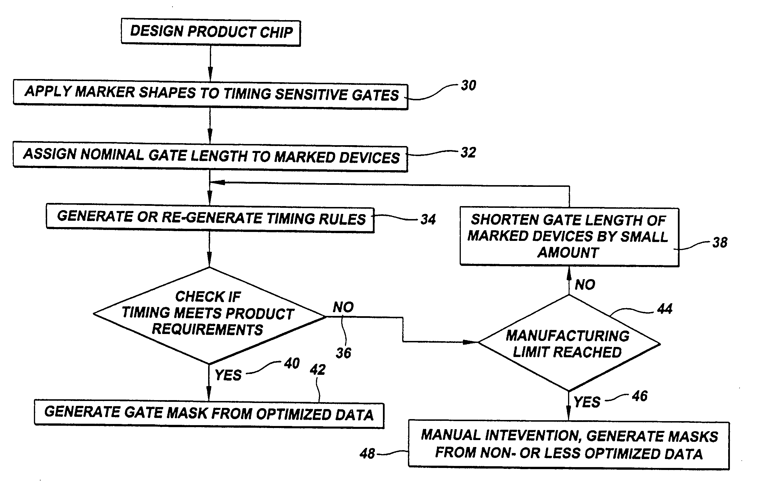
[0029] In a first embodiment, the present invention introduces a methodology for shortening L-poly, or trimming the gate lengths, for the devices in the critical path. This enables the transistors to switch ON at an earlier stage, and effectively lowers the device threshold voltage. The threshold voltage defines where each device approaches the conducting regime. If the threshold voltage is indeed lower, the transistor switches ON at an earlier time. For example, in an inverter stage, the inversion of the signal would be performed at an earlier time.

[0030] Shorting the L-poly of selected devices in the critical path makes each transistor switch faster. However, even though the switching speed is enhanced there remains the expected drawback, namely, with a lower threshold voltage, VT, comes an increase in leakage current for all the affected devices. In this manner, the devices that are not supposed to be conducting will generally leak more current, which cumulatively adds and yields...

second embodiment

[0036] In a second embodiment, the RC time constants of devices in the time-sensitive critical path are adjusted, directly altering the switching times for the critical devices. The iterative methodology employed to shorten the L-poly using OPC trimming may also be applied to adjust metal lines that form resistive paths, and to adjust the parasitic capacitance coupling among device neighbors.

[0037]FIG. 4 depicts the process flow of the methodology of the present invention for design a product chip for Front End-of-Line (FEOL) processing using the OPC trimming technique of the present invention. First, marker shapes are analytically applied to timing sensitive gates and BEOL paths 50. Normally, BEOL begins as the first contact for all metallization layers. BEOL suffers from RC delay due to long line lengths and next-neighbors. The resistance (R) may be improved by making the metallization line wider; however, this creates capacitive (C) issues. Nominal gate lengths are assigned to th...


PUM


Abstract

An iterative timing analysis is analytically performed before a chip is fabricated, based on a methodology using optical proximity correction techniques for shortening the gate lengths and adjusting metal line widths and proximity distances of critical time sensitive devices. The additional mask is used as a selective trim to form shortened gate lengths or wider metal lines for the selected, predetermined transistors, affecting the threshold voltages and the RC time constants of the selected devices. Marker shapes identify a predetermined subgroup of circuitry that constitutes the devices in the critical timing path. The analysis methodology is repeated as often as needed to improve the timing of the circuit with shortened designed gate lengths and modified RC timing constants until manufacturing limits are reached. A mask is made for the selected critical devices using OPC techniques.

Description

BACKGROUND OF THE INVENTION [0001] 1. Field of the Invention [0002] The present invention relates to semiconductor wafer processing, particularly to the enhancement of chip yield, performance, and timing. More particularly, the present invention relates to a methodology for modifying selected devices that affect the critical timing of the chip and developing a mask for optically trimming the gate lengths of the devices within the critical path. [0003] 2. Description of Related Art [0004] Optical Proximity Correction (OPC) is required when a different printing of a first feature occurs because a second feature is in close proximity to the first feature. The proximity of the second feature plays a role in altering the printing image of the first feature. In order to compensate for the impact coming from the closeness of other features, proximity features are adjusted in terms of their line width and length, particularly at the gate level. [0005] Devices in a circuit's critical path ne...

Claims


Application Information

Patent Timeline
Patent Type & Authority Applications(United States)
IPC IPC(8): G06F17/50
CPCG06F17/5068G06F30/39
Inventor CULP, JAMES A.LIEBMANN, LARS W.MALIK, RAJEEVMULLER, K. PAULNARASIMHA, SHREESHRUNYON, STEPHEN L.WILLIAMS, PATRICK M.
Owner GLOBALFOUNDRIES INC
Why Eureka
Try Eureka