Display device and manufacturing method of the same

Inactive Publication Date: 2007-05-17
SEMICON ENERGY LAB CO LTD
View PDF16 Cites 23 Cited by
  • Summary
  • Abstract
  • Description
  • Claims
  • Application Information

AI Technical Summary

Benefits of technology

[0032] By using the present invention, a low resistance material can be used as a wire, and the problem of signal delay in a large panel can be solved.
[0033] In addition, a low resistance material portion of a leading wire is not partially formed according to w

Problems solved by technology

Recently, with the increase in size of display panels, the problem of signal delay has been occurring, due to the increase in the length of wires (also referred to as a wiring) such as gate wires or source wires (also referred to as a gate wiring and a source wiring, respectively).
However, because copper is an element having mobility, when it is employed as a wire material, deterioration of a semiconductor element becomes a problem.
When a “damascene” method is adopted for manufacturing a panel, a polishing process (a planarization process) becomes a problem.
In an integrated circuit using a Si wafer, the wafer size is about 300 mmφ, while the glass substrate s

Method used


Image

  • Display device and manufacturing method of the same
  • Display device and manufacturing method of the same
  • Display device and manufacturing method of the same

Examples


embodiment mode 1

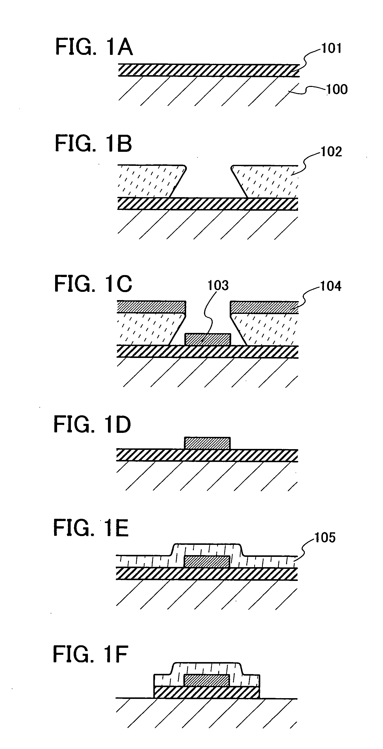
[0053] Embodiment Mode 1 will describe a manufacturing method of a wire using a low resistance material, with reference to FIGS. 1A to 1F.

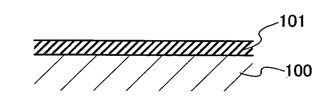
[0054] First, a first conductive film 101 serving as a barrier layer is formed over a surface 100 (hereinafter, also referred to as a formation surface) to be provided with a wire (FIG. 1A). As a material of the first conductive film 101, any of tungsten (W), molybdenum (Mo), chromium (Cr), titanium (Ti) and tantalum (Ta), which are high melting point materials, or an alloy thereof (e.g., W—Mo, Mo—Cr, or Ta—Mo), or a nitride thereof (e.g., tungsten nitride (WNx), titanium nitride (TiNx), tantalum nitride (TaNx), or TiSiNx), or the like can be used. A sputtering method, a CVD method or the like can be adopted as the formation method.

[0055] Then, a resist mask 102 is selectively formed over the first conductive film 101 (FIG. 1B). At this time, the resist mask 102 is selectively formed so as to expose a region in which a second conductive film 103...

embodiment mode 2

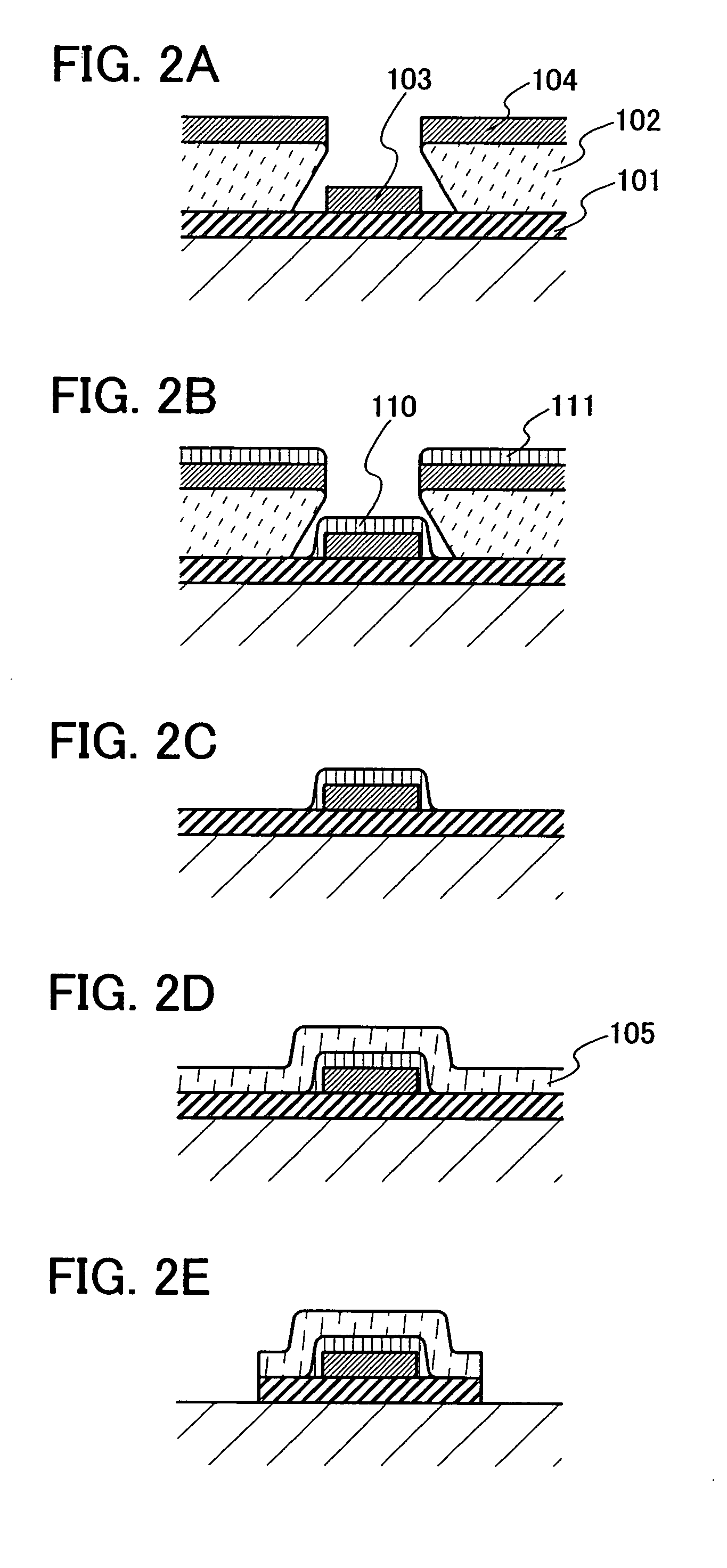
[0063] Embodiment Mode 2 will describe another mode of a manufacturing method of a wire using a low resistance material, with reference to FIGS. 2A to 2E.

[0064] As in Embodiment Mode 1, second conductive films 103 and 104 are formed over first conductive film 101 and a resist mask 102 (FIG. 2A). As a material of the first conductive film 101, any of tungsten (W), molybdenum (Mo), chromium (Cr), titanium (Ti), and tantalum (Ta), which are high melting point materials, or an alloy thereof (e.g., W—Mo, Mo—Cr, or Ta—Mo) or a nitride thereof (e.g., tungsten nitride (WNx), titanium nitride (TiNx), tantalum nitride (TaNx), or TiSiNx), or the like can be used. A sputtering method, a CVD method, or the like can be adopted as the formation method.

[0065] As the materials of the second conductive films 103 and 104, copper (Cu) is preferable; however, there is no particular limitation as long as they are low resistance materials. For example, silver (Ag), aluminum (Al), gold (Au), an alloy the...

embodiment mode 3

[0073] Embodiment Mode 3 will describe a manufacturing method of a bottom-gate type thin film transistor (hereinafter referred to as a TFT) using a low resistance material as a wire, with reference to FIGS. 3A to 3F and 4A to 4E.

[0074] A wire 201 serving as a gate electrode is formed over a substrate 200 by the method shown in Embodiment Mode 1 (FIG. 3A). A thickness of the wire 201 is preferably 10 nm to 200 nm. The wire 201 includes a stacked structure of a first conductive film 201a, a second conductive film 201b, and a third conductive film 201c. In this embodiment mode, the second conductive film 201b formed from a low resistance material is not formed in a region which is to become a gate electrode later. In other words, the second conductive film 201b corresponding to the second conductive film 103 shown in FIG. 1F is not shown in FIGS. 3A to 3F and 4A to 4E, which show a cross-section of the thin film transistor. On the other hand, as shown in FIG. 4E, which is a top view, ...


PUM

PropertyMeasurementUnit
Angleaaaaaaaaaa
Angleaaaaaaaaaa
Lengthaaaaaaaaaa

Abstract

A plurality of wires and electrodes are formed by forming a first conductive film, selectively forming a resist over the first conductive film, forming a second conductive film over the first conductive film and the resist, removing the second conductive film formed over the resist by removing the resist, forming a third conductive film so as to cover the second conductive film formed over the first conductive film, and selectively etching the first conductive film and the third conductive film. Thus, wires using a low resistance material can be formed in a large-sized panel, and thus, a problem of signal delay can be solved.

Description

BACKGROUND OF THE INVENTION [0001] 1. Field of the Invention [0002] The present invention relates to a display device and a manufacturing method of the display device, specifically, a wire technology for the display device. [0003] 2. Description of the Related Art [0004] In recent years, flat panel displays (FPDs) typified by liquid crystal display (LCD) devices or electroluminescence (EL) display devices have been attracting attention as display device substitutes for CRTs (Cathode Ray Tubes). In particular, development of a large-screen liquid crystal television set mounted with a large liquid crystal panel which is driven with an active matrix method is the primary task for liquid crystal panel manufacturers. Further, EL televisions having a large screen have been developed actively. [0005] Conventionally, aluminum (Al) is mainly used as a wire material in a liquid crystal display device or an electroluminescence display device. Recently, with the increase in size of display pane...

Claims


Application Information

Patent Timeline
IPC IPC(8): G03C5/00
CPCH01L27/3279H01L51/0023H01L51/055H01L27/1288H01L29/4908H01L27/124H01L51/56H10K59/1315H10K71/621H10K10/481H10K71/00
Inventor FUJIKAWA, SAISHIHOSOYA, KUNIO
Owner SEMICON ENERGY LAB CO LTD
Why Eureka
Try Eureka