Group-III nitride semiconductor device

a semiconductor and nitride technology, applied in the direction of semiconductor lasers, semiconductor laser structural details, lasers, etc., can solve the problems of reducing the emission efficiency of semiconductor light-emitting devices, difficulty in growing crystals of high quality, and failure to obtain blue light of high emission intensity, so as to achieve enhanced emission intensity, low dislocation density, and suppression of light absorption

Active Publication Date: 2007-06-07
TOYODA GOSEI CO LTD
View PDF13 Cites 12 Cited by
  • Summary
  • Abstract
  • Description
  • Claims
  • Application Information

AI Technical Summary

Benefits of technology

[0025] According to the present invention, there is obtained a semiconductor element which comprises a thick AlGaN layer having low dislocation density and containing no cracks, and which does not include a thick GaN layer. Since the semiconductor element does not include a thick GaN layer, when an ultraviolet light-emitting device is produced from the semiconductor element, light absorption can be suppressed, and emission intensity is enhanced.
[0026] The semiconductor element does not require any treatment after growth of the AlGaN layer, and thus the element can be produced at high productivity.

Problems solved by technology

However, in the case where a GaN semiconductor layer is formed directly on a sapphire substrate, blue light of high emission intensity fails to be obtained, since the GaN semiconductor layer exhibits very poor crystallinity and surface morphology.
In the case of an AlGaN semiconductor layer, difficulty is encountered in growing crystals of high quality, as compared with the case of a GaN semiconductor layer, which is generally employed in, for example, a blue LED.
Therefore, when a semiconductor light-emitting device (i.e., an ultraviolet LED) is produced from the semiconductor element, the resultant semiconductor light-emitting device exhibits lowered emission efficiency; i.e., the device fails to attain intended characteristics.
However, in the case where an AlGaN layer is grown on a thick GaN layer, since the lattice constant of GaN differs from that of AlGaN, once the elastic limit has been surpassed, cracking occurs in the AlGaN layer.
Therefore, difficulty is encountered in growing crack-free crystals of high quality.
Particularly when the mol fraction of AlN in the AlGaN layer or the thickness of the AlGaN layer is increased, such cracking may become considerable.
When an LED is produced from the thus-formed semiconductor structure, the light absorption effect of the thick GaN layer would cause problems.
Meanwhile, removal of the thick GaN layer and the sapphire substrate after growth of the AlGaN layer leads to very poor productivity.

Method used


Image

  • Group-III nitride semiconductor device
  • Group-III nitride semiconductor device
  • Group-III nitride semiconductor device

Examples


example 1

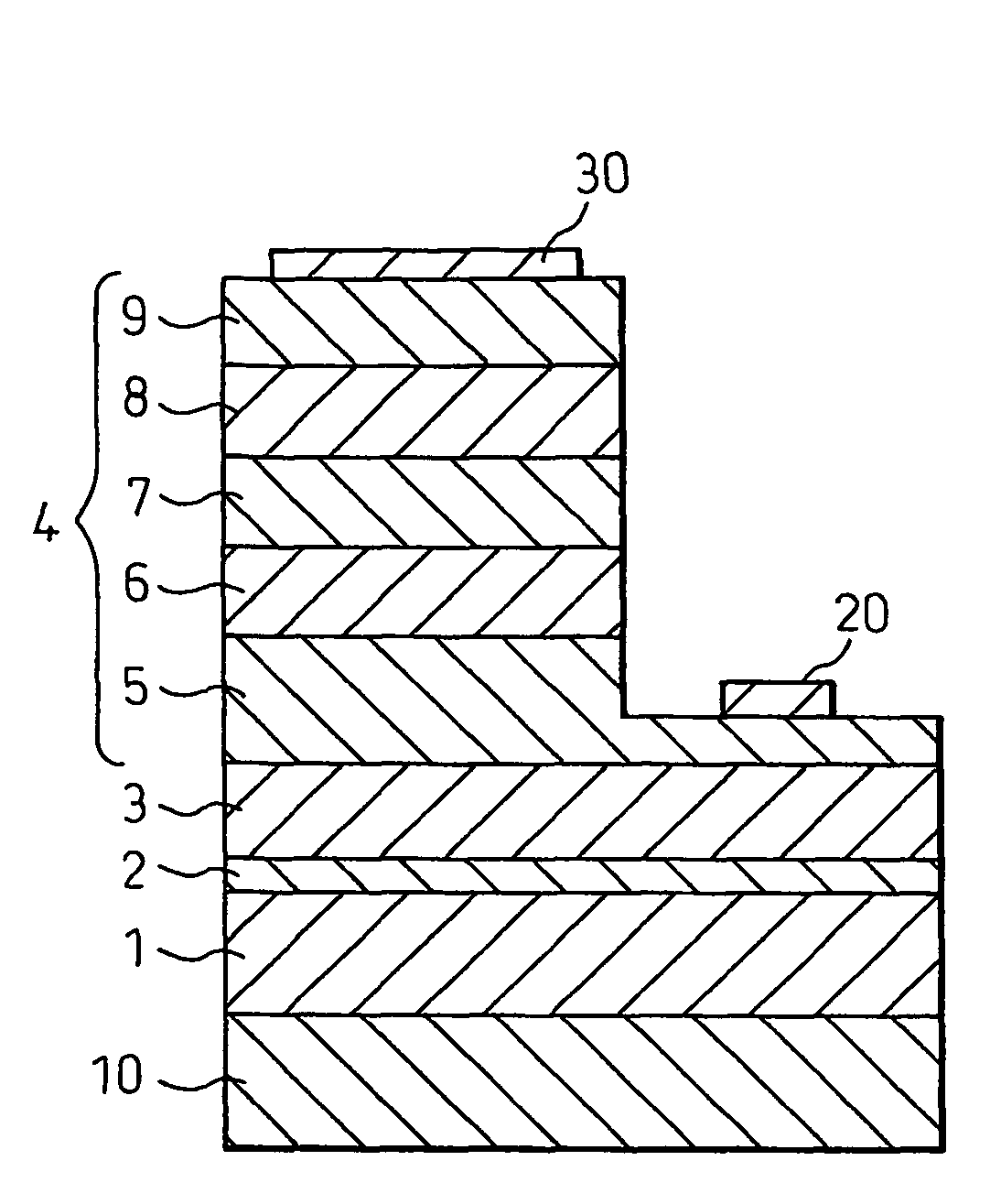
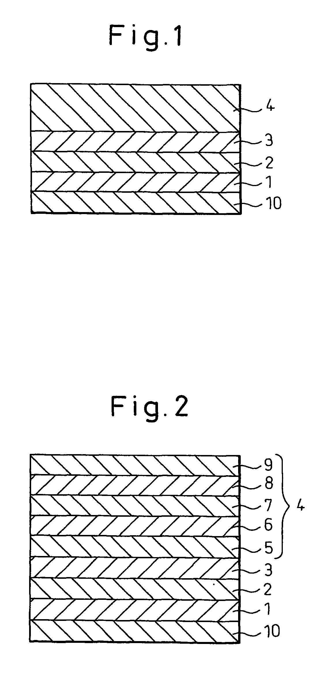
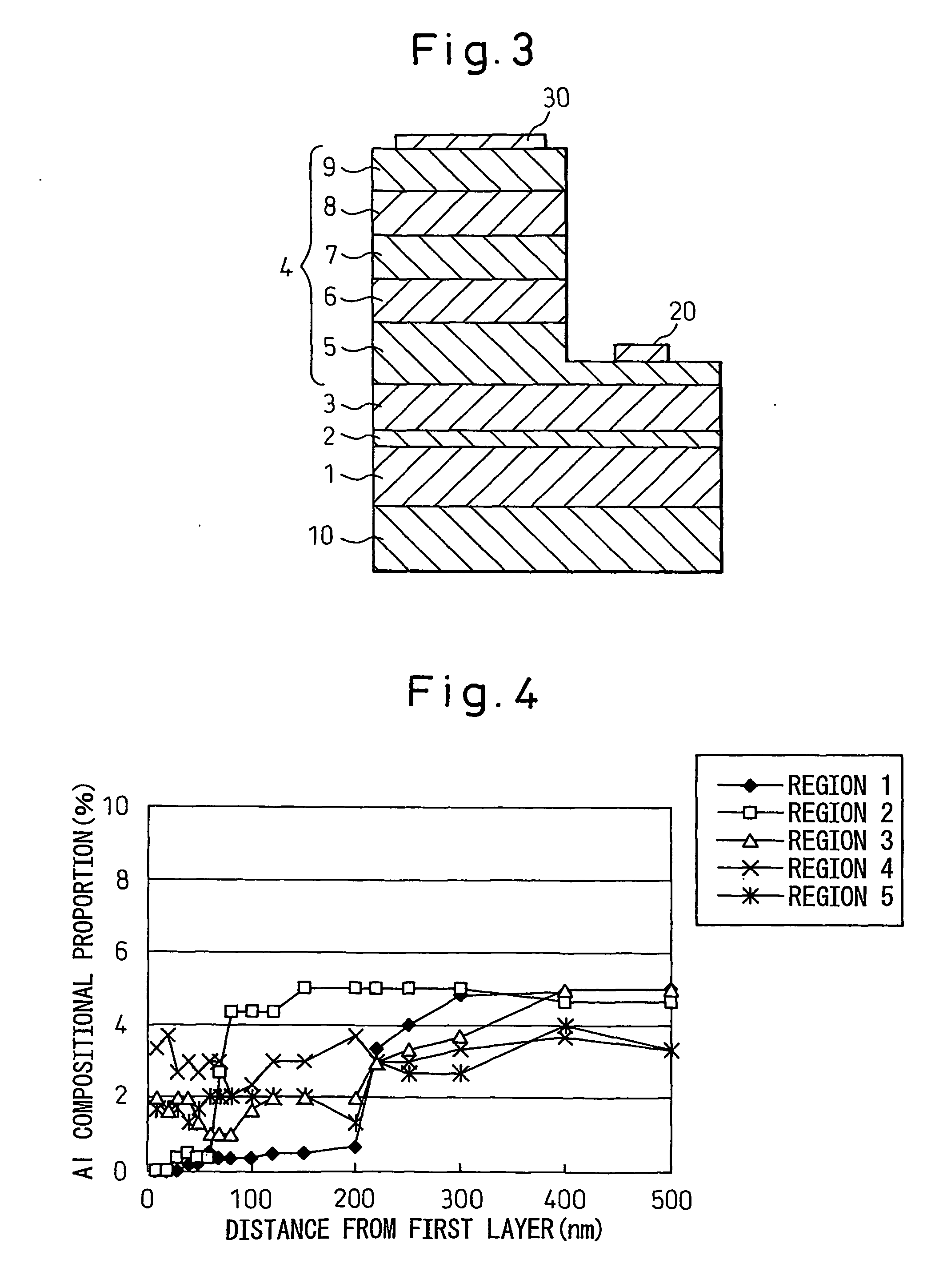
[0066]FIG. 3 is a schematic cross-sectional view showing the structure of the Group III nitride semiconductor light-emitting device produced in the present Example. The Group III nitride semiconductor light-emitting device shown in FIG. 3 was produced by successively forming semiconductor layers atop a sapphire substrate 10 through a well known MOCVD technique. The substrate 10 is a C-plane sapphire substrate having an off-angle of 0.2°. The sapphire substrate was placed in a reactor of an MOCVD growth furnace, and maintained in a hydrogen atmosphere at 1,000° C. for 10 minutes, thereby cleaning the sapphire substrate.

[0067] Subsequently, the temperature of a susceptor was increased to 1,180° C., and TMA (serving as an Al source) and NH3 (serving as an N source) were fed into the growth furnace, to thereby grow a first nitride semiconductor layer 1 formed of AlN. Specifically, H2 (serving as a carrier gas) (22 l / minute), NH3 (0.5 l / minute), and TMA (80 μmol / minute) were fed into th...

example 2

[0076] In the present Example, a low-temperature AlN buffer layer was employed as the first nitride semiconductor layer 1. The temperature of the susceptor was regulated to 500° C., and TMA and NH3 were fed into the MOCVD growth furnace, to thereby form the AlN buffer layer. Specifically, H2 (serving as a carrier gas) (22 l / minute), NH3 (0.5 l / minute), and TMA (80 μmol / minute) were fed into the MOCVD growth furnace, and the pressure in the growth furnace was regulated to 15 kPa, to thereby form the AlN buffer layer having a thickness of about 30 nm. The procedure of Example 1 was repeated, except that the thus-formed AlN buffer layer was employed as the first nitride semiconductor layer 1, to thereby produce a light-emitting diode device. The resultant light-emitting diode device exhibited characteristics comparable to those of the light-emitting diode device of Example 1.


PUM

PropertyMeasurementUnit
thicknessaaaaaaaaaa
thicknessaaaaaaaaaa
thicknessaaaaaaaaaa

Abstract

An object of the present invention is to provide a Group III nitride semiconductor element which comprises a thick AlGaN layer exhibiting high crystallinity and containing no cracks, and which does not include a thick GaN layer (which generally serves as a light-absorbing layer in an ultraviolet LED).
The inventive Group III nitride semiconductor element comprises a substrate; a first nitride semiconductor layer composed of AlN which is provided on the substrate; a second nitride semiconductor layer composed of Alx1Ga1-x1N (0≦x1≦0.1) which is provided on the first nitride semiconductor layer; and a third nitride semiconductor layer composed of Alx2Ga1-x2N (0<x2<1 and x1+0.02≦x2) which is provided on the second nitride semiconductor layer.

Description

CROSS REFERENCE TO RELATED APPLICATION [0001] This application is an application filed under 35 U.S.C. §111(a) claiming benefit pursuant to 35 U.S.C. §119(e) (1) of the filing date of the Provisional Application No. 60 / 513,596 filed on Oct. 24, 2003, pursuant to 35 U.S.C. §111(b).TECHNICAL FIELD [0002] The present invention relates to a Group III nitride semiconductor element employed in electronic devices, including light-emitting devices such as a light-emitting diode (LED) and a laser diode (LD), light-receiving devices such as an optical sensor, and transistors. More particularly, the present invention relates to a Group III nitride semiconductor element useful for producing light-emitting devices which emit ultraviolet light (i.e., light having a wavelength of 380 nm or less). BACKGROUND ART [0003] GaN (gallium nitride) compound semiconductors have already been put into practical use in, for example, blue light-emitting diodes (LEDs). In general, a GaN compound semiconductor is...

Claims


Application Information

Patent Timeline
Patent Type & Authority Applications(United States)
IPC IPC(8): H01L33/00H01L21/20H01L21/205H01L29/20H01L29/205H01L33/12H01L33/32H01S5/02
CPCH01L21/0237H01L21/0242H01L21/02458H01L21/02502H01L21/0254H01L21/02576H01L21/02579H01L21/0262H01L29/2003H01L29/205H01L31/184H01L33/007H01L33/12H01L33/32H01S5/32341H01S2301/173H01S2304/04
Inventor SAKAI, HIROMITSUOKUYAMA, MINEO
Owner TOYODA GOSEI CO LTD
Why Eureka
Try Eureka