Semiconductor nanoparticle surface modification method

a technology of semiconductor nanoparticles and surface treatments, applied in the field of semiconductor nanoparticles, can solve the problems of insufficient durability of semiconductor nanoparticles subjected to surface treatment, such as oh coating or ammonia treatment, and cannot be used in luminescent compositions, instruments, and other directions

Inactive Publication Date: 2007-06-14
HITACHI LTD
View PDF25 Cites 72 Cited by
  • Summary
  • Abstract
  • Description
  • Claims
  • Application Information

AI Technical Summary

Benefits of technology

[0030] According to the present invention, semiconductor nanoparticles that are available for use in industries related to bio-applications can be synthesized. Further, reagents that are relatively safer than those used in existing methods ca

Problems solved by technology

However, semiconductor nanoparticles that have been subjected to a surface treatment, such as an OH coatin

Method used


Image

  • Semiconductor nanoparticle surface modification method
  • Semiconductor nanoparticle surface modification method
  • Semiconductor nanoparticle surface modification method

Examples


example 1

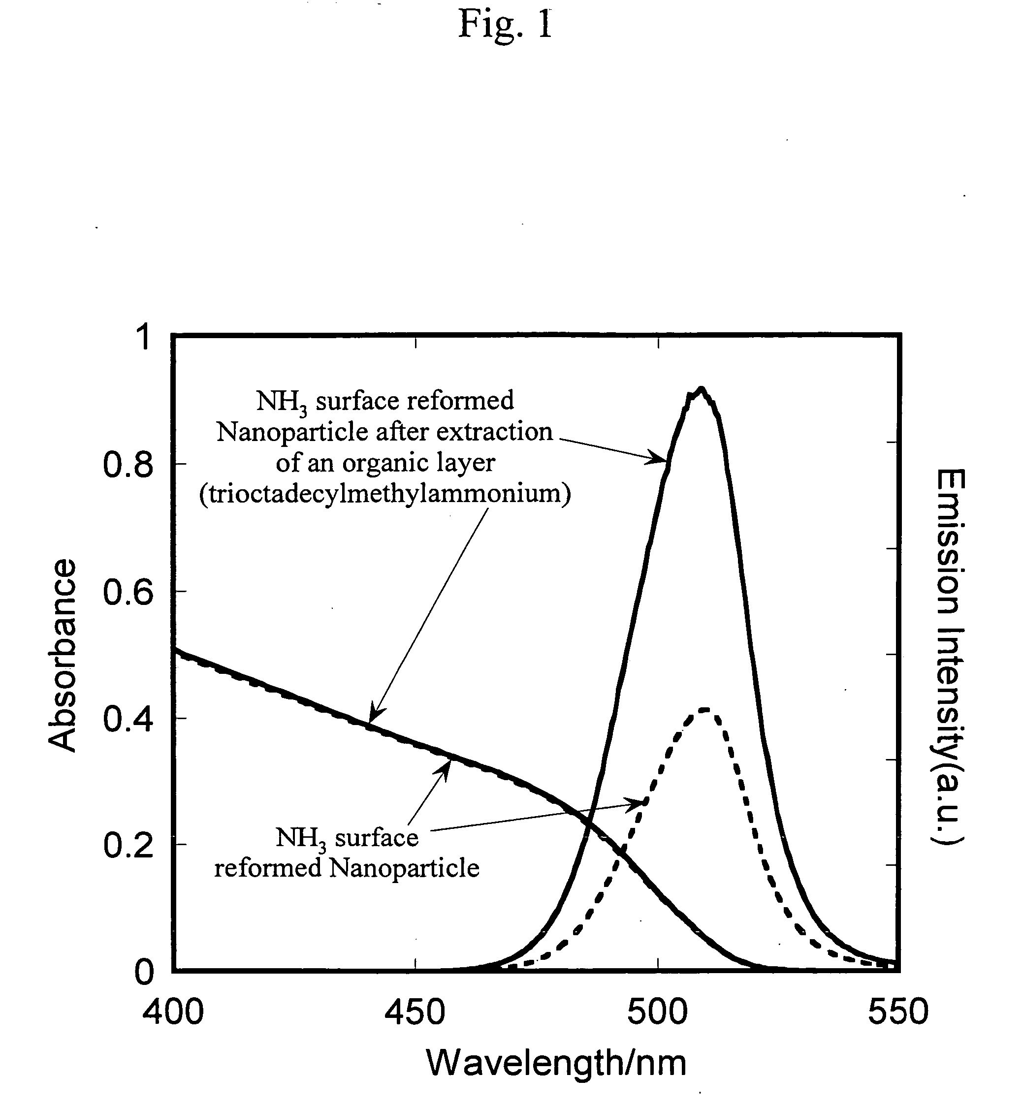
[0044] Nanoparticles perfectly dispersed into the organic solvent obtained as mentioned above were coated with amphipathic molecules. 10 ml of a solution in which nanoparticles had perfectly dispersed into the aforementioned organic solvent was put into a container such as a stoppered test tube or an eggplant shaped flask, etc. and was made to assume a membranous form on the inner wall of the container by evaporation. Then, the particles were dissolved again by adding 2 ml of solution in which dodecyltrimethylammonium chloride was dissolved in chloroform to a concentration of 5 mM, and the resulting solution was made to assume a membranous form again on the inner wall of the container by evaporation. Moreover, after removing residual chloroform by heating the container at 90° C., the particles were dissolved again by adding 2 ml of methanol. Then, methanol was removed by adding 10 ml of ultrapure water, followed by agitation for some time during heating to 90° C. Finally, an optical...

example 2

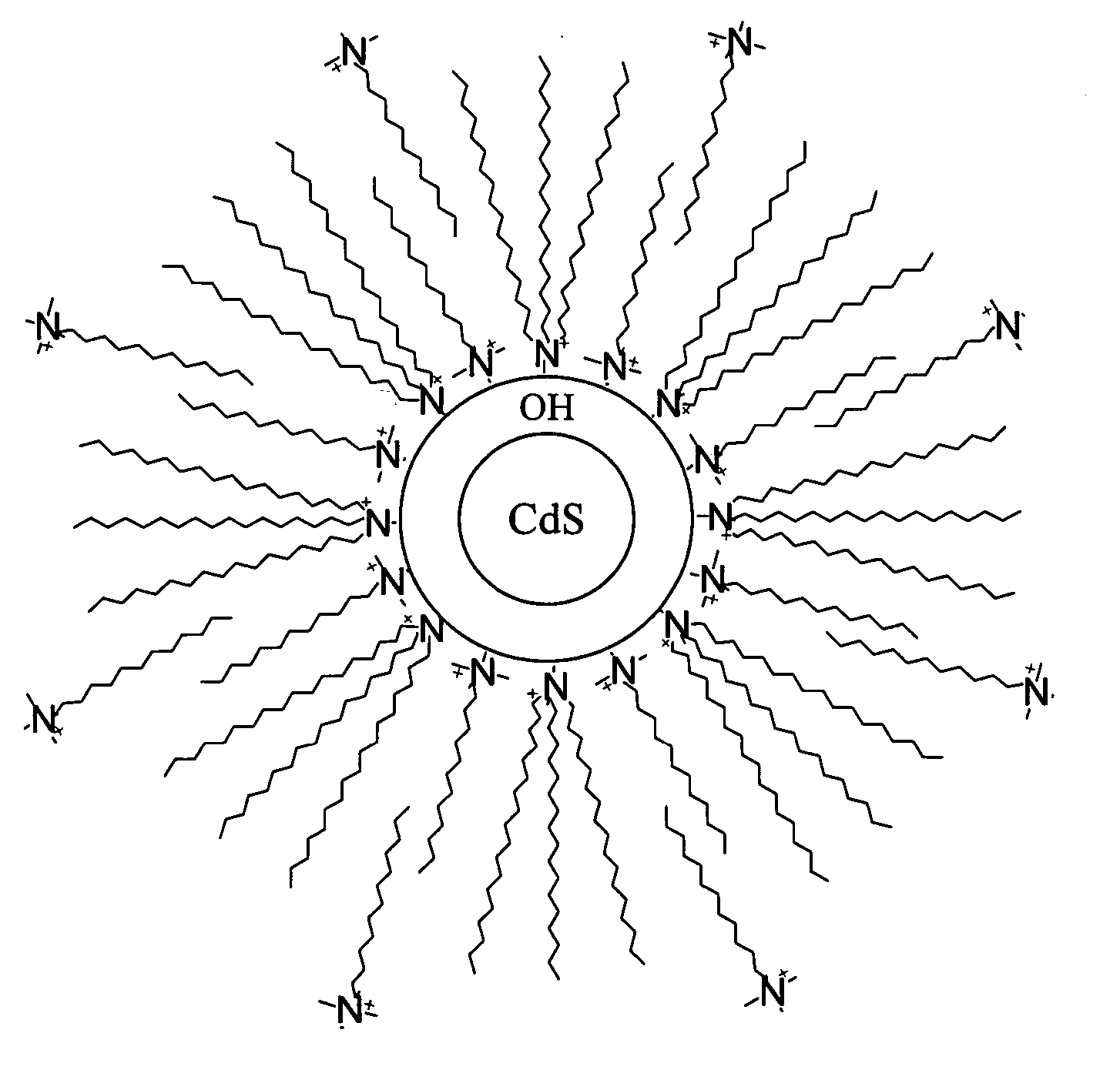
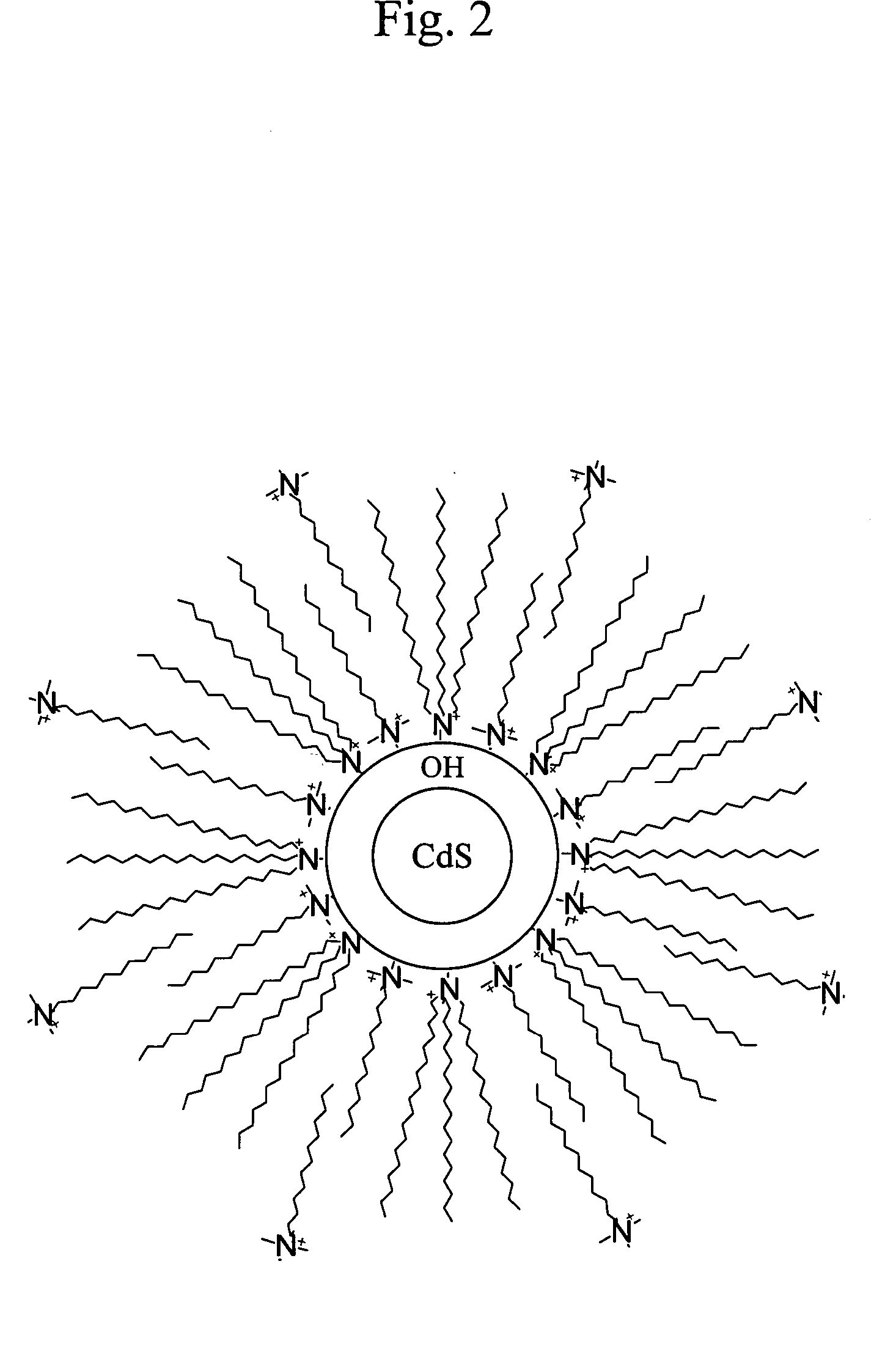
[0047] CdS nanoparticles perfectly dispersed into the organic solvent obtained as mentioned above (10 ml) were put into an eggplant shaped flask, and then hexane was removed by evaporation. 2 ml of chloroform was added and octadecylamine was added thereto to a concentration of 0.5 mM, and then, they were dissolved using ultrasonic wave. Further, the chloroform was removed by evaporation, and 2 ml of THF was added thereto for dissolving the nanoparticles again. Here, ultrasonic treatment may be used. Then, 10 ml of ultrapure water and a stirring bar were put into an eggplant shaped flask, and CdS nanoparticles dissolved in THF were rapidly poured thereto while agitated by the stirrer. The solution was dissolved by ultrasonic treatment, etc, only THF was removed by evaporation for obtaining a water solution, and then, the water solution was put into a centrifuge tube for removing precipitation by centrifugation. Thereby, water-soluble nanoparticles with amino groups arranged on the su...


PUM


Abstract

Semiconductor nanoparticles having high luminescence properties that are preferable for applications and uses of biotechnology are provided. With the use of electric charges on the surfaces of particles, the particles and selected polymers are allowed to electrostatically bind to each other, such that the surfaces of the particles are coated. The polymers are allowed to crosslink to each other, resulting in the improved durability of the particles. Further, functional groups contained in the polymers are exposed on the surfaces of the particles. Accordingly, semiconductor nanoparticles that are preferably utilized for applications such as staining and labeling of biopolymers have been synthesized.

Description

CROSS-REFERENCE TO RELATED APPLICATION [0001] This application is a Continuation-in-Part application of U.S. application Ser. No. 11 / 325,533 filed Jan. 5, 2006. Priority is claimed based on U.S. application Ser. No. 11 / 325,533 filed Jan. 5, 2006, which claims the priority of Japanese Patent Application No. 2005-001583 filed on Jan. 6, 2005, all of which is incorporated by reference.BACKGROUND OF THE INVENTION [0002] 1. Field of the Invention [0003] The present invention relates to a semiconductor nanoparticle having high luminescence properties and a method for synthesizing the same. Moreover, the present invention relates to a fluorescent reagent and an optical device comprising such semiconductor nanoparticle. [0004] 2. Background Art [0005] Semiconductor nanoparticles with particle sizes of 10 nm or less are located in the transition region between bulk semiconductor crystals and molecules, so that they exhibit physicochemical properties different from those of either bulk semico...

Claims


Application Information

Patent Timeline
IPC IPC(8): C09K11/06
CPCB82Y30/00C01G9/08C01G11/02C01P2004/04C01P2004/64C01P2006/40C01P2006/60C09C1/12C09C1/3072C09C1/3676C09C3/10C09K11/565C09K11/62C09K11/64C09K11/66C09K11/70C09K11/74C09K11/75C09K11/88C09K2211/14G01N33/54346Y10S977/773Y10S977/902
Inventor SATO, KEIICHIHATTORI, SHINYACHIBA, TAEKO
Owner HITACHI LTD
Why Eureka
Try Eureka