
Methods for chemically treating a substrate using foam technology

a technology of chemical treatment and substrate, applied in the direction of detergent compounding agents, cleaning using liquids, instruments, etc., can solve the problems of reducing the ultimate product performance, affecting the manufacturing process, and forming post-etch residues (per), so as to reduce undesired oxidation reactions, prevent adsorption and readsorption of metals, and increase safety

Inactive Publication Date: 2007-06-14
EKC TECH
View PDF38 Cites 23 Cited by
  • Summary
  • Abstract
  • Description
  • Claims
  • Application Information

AI Technical Summary

Benefits of technology

The present invention provides foam compositions and methods for cleaning, rinsing, and etching substrates. The foams are selective in removing organic and inorganic compounds, including post-etch residue, and can operate at low temperatures. The foam compositions contain a gas, a surfactant, deionized water, and a component selected from the group consisting of a fluoride, a hydroxylamine, an amine, and periodic acid. The foams can also contain chelating agents and corrosion inhibitors to prevent metal adsorption and oxidation reactions. The foams have a synergistic cleaning effect and can remove undesired matter from the surface of a substrate through bubble formation, scrubbing, and bubble bursting. The foam processes are safer, require less potentially hazardous chemical, and provide increased safety, decreased material costs, and increased product performance compared to liquid-based techniques. The foams are particularly effective in removing post-etch residue from semiconductor substrates without affecting structural integrity and detail.

Problems solved by technology

Contamination of the surface of the substrate with undesired matter can affect the manufacturing process and reduce ultimate product performance.
However, the disadvantage to dry etching is the formation of post-etch residue (PER), which is a difficult to remove by-product of the reaction between the plasma, the substrate surface, and other material present such as the photoresist.
Combining high temperatures with an easily ignitable rinse is clearly less than desirable.
Planarization improves the contact between the wafer, the dielectric insulators, and the metal substrates, but also increases the room for error in other process steps.
At dimensions of 0.10 microns and less, most semiconductor substrates will need to use conductive materials with low dielectric constants (low-k materials), and such materials are inherently delicate.
For example, an amine based cleaning agent can leave trace amounts of amine, which may be corrosive to metal substrates such as aluminum.
However, as previously mentioned, the flammability of such solvents is a disadvantage.
Dilute HF is commonly used to remove the remaining monolayer amounts of organic or inorganic contaminants including metals and anions, but unlike organic chemistries, even dilute HF can damage the semiconductor substrate if not carefully controlled.
It has been found, however, that megasonics is only effective at removing particles as small 0.3 microns and is not expected to be effective at removing particles that are an order of magnitude smaller.
However, foam compositions utilizing non-aqueous solvents in combination with cleaning chemicals were not disclosed.
Furthermore, foam techniques for removal of post-etch residue, or for carrying out CMP, were not taught.
Although carbon dioxide has a surface-tension reducing effect on an aqueous solution, at higher concentrations it produces an acidic solution and may not be compatible with other cleaning reagents.
A disadvantage of using foam was that the foam must remain stable and in contact with the substrate long enough to deliver cleaning chemical.
Nevertheless, although an advantage of foam compositions and processes is that less liquid and chemical is necessary to achieve the same amount of cleaning as that achieved using liquid phase semiconductor cleaning, etching, and rinsing technology, formulating effective foam chemistries is difficult.
Unpredictable criteria such as effective means of foam production and stability militate against universal applicability of foam techniques, however.
A further principal disadvantage of current foam technology is that it doesn't provide methods and foam compositions for chemicals that are capable of cleaning post-etch residue.

Method used


Image

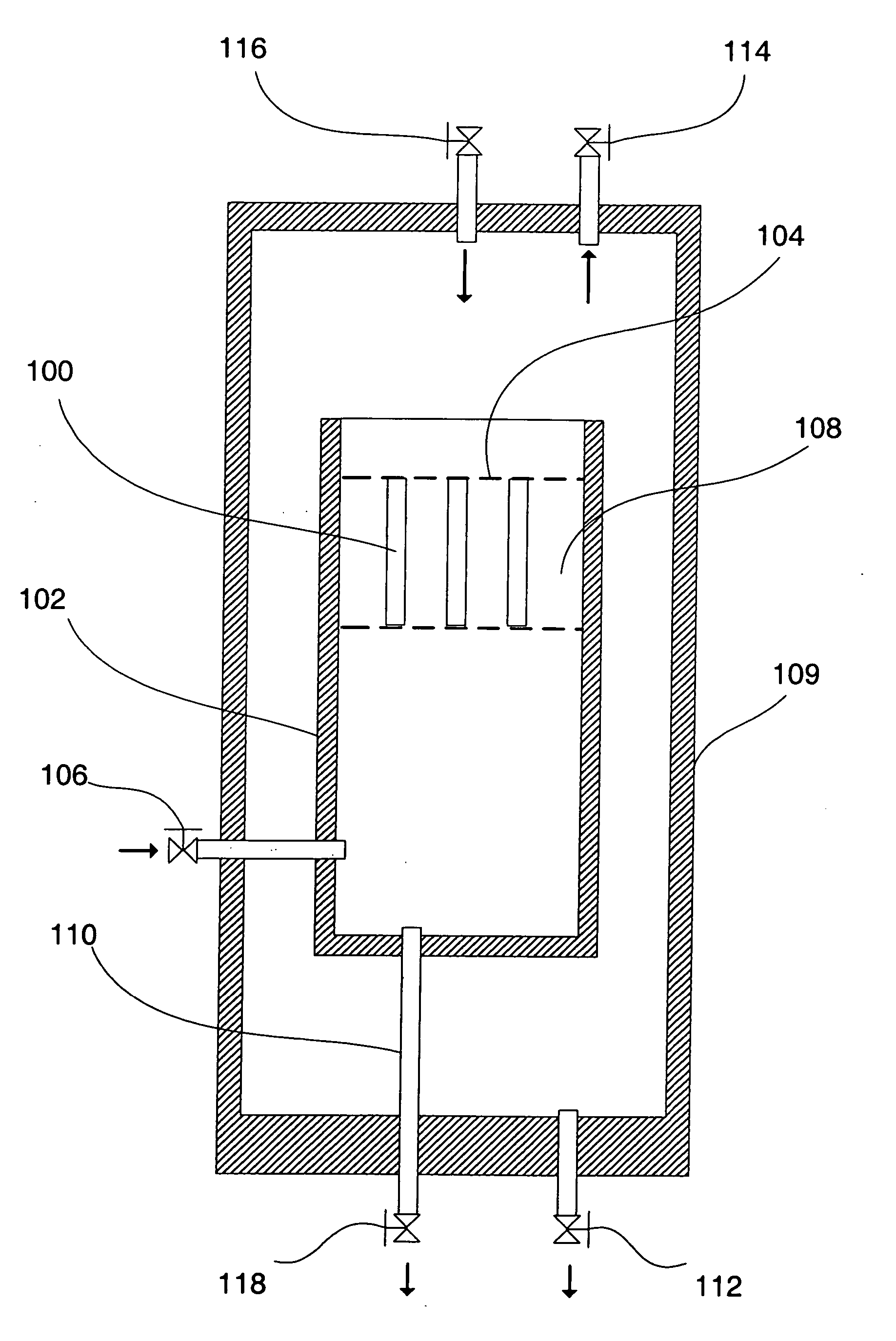
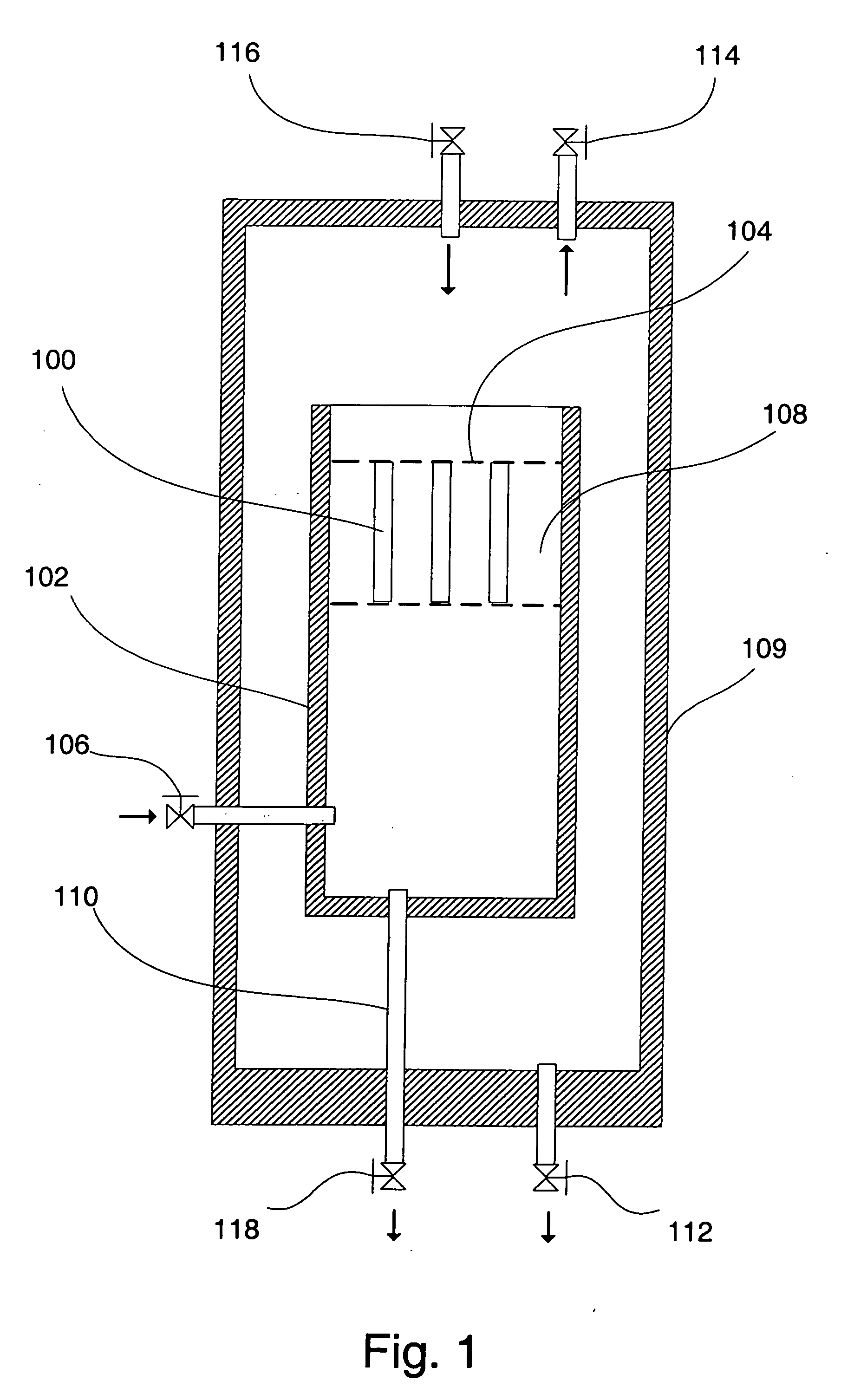
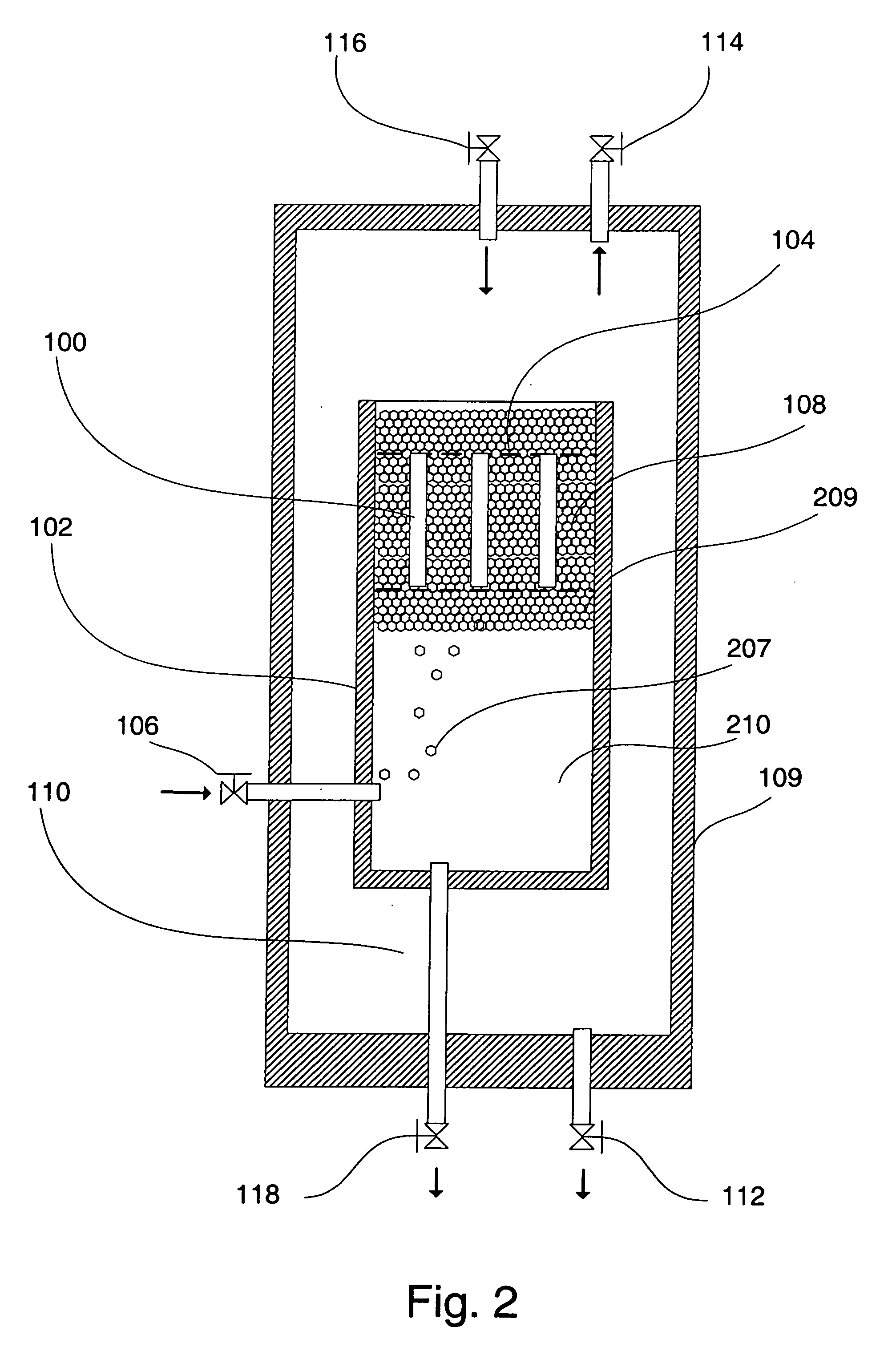
  • Methods for chemically treating a substrate using foam technology
  • Methods for chemically treating a substrate using foam technology
  • Methods for chemically treating a substrate using foam technology

Examples


example 1

Fluoride-Based Compositions in Cleaning.

[0117] Liquid phase cleaning of a substrate was compared to foam phase cleaning. The cleaning chemical concentration was the same in both the liquid and foam experiments. Two different proprietary wafers were used in these cleaning experiments. Each wafer surface was contaminated with post-etch residue from the previous removal process. The wafers were designated T and S. Two surfactants were used to make the compositions foamable: a sodium salt of dodecylbenzene sulfonic acid (anionic surfactant, obtained from Aldrich Chemical Co, Milwaukee, Wis.) and NCW601A (nonionic surfactant, obtained from Waco Chemical, Richmond, Va.).

[0118] The liquid phase cleaning experiments involved suspending a wafer fragment in a 100 cm3 beaker and stirring the cleaning composition magnetically at room temperature and pressure for a designated time. The foam phase cleaning experiments involved suspending a wafer fragment in a tall cylindrical vessel equipped wi...

example 2

Hydroxylamine Based Compositions

[0124] Table 3 provides examples chemical formulations capable of foaming with surfactants with each component expressed in weight percent prior to addition of surfactant.

TABLE 3Some HDA Cleaning Formulations Capable of Foaming2-methylamineGallicHydroxylamineDiglycol amineDIethanol (MAE)CatecholAcidFormulawt %wt %wt %wt %wt %wt %D35605E3055510F3027.5527.510G264817.58.5

Formulations D, E, F and G additionally contain an amount of a surfactant sufficient to ensure foaming at desired operating temperatures.

example 3

Copper-compatible Chemistries

[0125] Some copper compatible cleaning formulations that are capable of foaming, along with variations in those formulations are provided in the Tables 4 and 5.

TABLE 4Some Copper Compatible Cleaning Formulationsfor Use in Foaming-based CleaningTempTimeFormulaComposition / Weight %(C.)(min)H40-60% morpholine, 20-50% N-methyl45-855-60pyrrolidone, 5-25% γ-butylolactoneI5-45% choline, 1-10% hydroxylamine,35-855-6060-90% deionized waterJ1-10% 2-methylamine ethanol, 20-50%45-1055-60N-methyl pyrrolidone, 50-90% dimethylsulfoxideK10-50% choline, 20-80% propylene35-855-60glycol, ˜25% deionized water.

It is noted that formulations H and J in Table 4 do not have deionized water in them. All of formulations H through J additionally contain an amount of a surfactant sufficient to ensure foaming.

[0126]

TABLE 5Other Copper Compatible Cleaning Formulations for Use in Foaming Technologies.TABLE 5AHWeight %EXISTINGOTHERSamine40-60morpholinemonoethanolamine, diglycol amine,...


PUM

PropertyMeasurementUnit
weight percentaaaaaaaaaa
operating temperaturesaaaaaaaaaa
temperaturesaaaaaaaaaa

Abstract

The present invention relates to methods and compositions for treating a surface of a substrate by foam technology that includes at least one treatment chemical. The invention more particularly relates to the removal of undesired matter from the surface of substrates with small features, where such undesired matter may comprise organic and inorganic compounds such as particles, films from photoresist material, and traces of any other impurities such as metals deposited during planarization or etching. A method according to the present invention for treating a surface of a substrate comprises generating a foam from a liquid composition, wherein the liquid composition comprises a gas; a surfactant; and at least one component selected from the group consisting of a fluoride, a hydroxylamine, an amine and periodic acid; contacting the foam with the surface of a substrate; and, removing the undesired matter from the surface of the substrate.

Description

FIELD OF THE INVENTION [0001] The present invention relates to methods and compositions for chemically treating a surface of a substrate by using foam technology. The invention more particularly relates to the removal of organic and inorganic compounds such as photoresist and post-etch residue from substrate surfaces. BACKGROUND OF THE INVENTION [0002] A substrate is an underlying solid material used in manufacturing products such as integrated electronic circuitry and microelectromechanical systems (MEMS). MEMS result from a technological advancement that unites silicon-based microelectronics with micromachining technology with the goal of producing complete systems on a single chip. [0003] Integrated circuit and MEMS manufacturing comprise stepwise patterning and layering processes. Examples of such processes include the use of plasma to etch circuit-defining pathways, deposition of metals in the pathways to form circuitry, and application of chemicals and abrasives to etch, strip...

Claims


Application Information

Patent Timeline
Patent Type & Authority Applications(United States)
IPC IPC(8): C11D7/32C11D3/02C11D3/20C11D3/26C11D3/28C11D3/30C11D3/32C11D3/33C11D3/34C11D3/43C11D11/00C23F3/06
CPCC11D3/0094C11D3/046C11D3/2058C11D3/2075C11D3/2082C11D3/2086C11D3/26C11D3/28C11D3/30C11D3/32C11D3/33C11D3/3445C11D3/43C11D11/0047C23F3/06C11D2111/22
Inventor PATEL, BAKUL P.CERNAT, MIHAELA ANCA-MACSMALL, ROBERT J.
Owner EKC TECH
Learn More