Plasma Processing Apparatus And Plasma Processing Method

a plasma processing apparatus and plasma technology, applied in the direction of chemical vapor deposition coating, coating, electric discharge tube, etc., can solve the problems of deteriorating lsi circuit performance, inability to perform long-term stable processing, chemical eroded inner wall material of the reaction chamber, etc., to prevent the increase of wall damage caused by ion sputtering and suppress plasma potential.

Inactive Publication Date: 2007-08-02
HITACHI LTD +1
View PDF9 Cites 3 Cited by
  • Summary
  • Abstract
  • Description
  • Claims
  • Application Information

AI Technical Summary

Benefits of technology

[0021] The present invention aims at solving the problems of the prior art mentioned above. In other words, the object of the present invention is to provide a plasma processing apparatus and plasma processing method capable of reducing the amount of impurities in the reaction chamber without deteriorating the stability of plasma.
[0026] According to the present invention, when a base material of the DC earth is composed of a non-metallic material such as conductive ceramic, SiC, Al or Al compound, a conductive member having a conductivity of 1 Ωcm or less is disposed on the mounting surface of the DC earth by evaporation, spraying or interposing, thereby reducing the earth resistance of the DC earth.
[0027] According to the present structure, even if the inner wall is coated with a chemically stable protective coating so as to reduce the amount of metal impurities generated from the metal inner wall material of the plasma reaction chamber, the plasma near the inner wall is earthed in DC-like manner, so the plasma is prevented from becoming unstable, and the LSI circuits will not be damaged. Further, as shown in FIG. 9, since the DC earth provides an earth at a position where the plasma potential øp is high, the plasma potential at the inner wall portion and at the earth portion of the reaction chamber can be reduced. Thus, the voltage accelerating the ions in the plasma can be cut down, and the wall damage caused by ion sputtering can be suppressed.
[0029] Therefore, by disposing the DC earth at a location closer to the plasma generating region (where plasma density is highest) than the position of the earth portion (inner wall of the reaction chamber) or at the inner wall of the reaction chamber where wall sputtering must be suppressed, the plasma potential at the inner wall or at the earth portion where sputtering becomes a problem can be reduced by δV.
[0030] By providing as the protective coating of the inner wall of the reaction chamber an insulating ceramic such as carbide, oxide or nitride like SiC, boron carbide and alumite, and the thickness d of the dielectric coating is determined so that, with respect to the relationship between frequency f of the high frequency applied to the substrate and the dielectric constant ∈ of the dielectric, an impedance per unit area R=d / (2πf∈) when the high frequency is propagated by capacity coupling through the dielectric portion is 100Ω or smaller, the impedance R of the protective coating is maintained low with respect to high frequencies, so the coating does not deteriorate the function of the earth to high frequencies. As a result, even when the inner wall of the reaction chamber is covered with protective coating, the impedance of the protective coating with respect to the high frequency current flowing into the wall or the earth portion is increased, by which the variation in the plasma potential can be suppressed, and the increase of wall damage caused by ion sputtering can be prevented.

Problems solved by technology

In a plasma etching apparatus, for example, high frequency is applied to the wafer to be processed using reactive gas plasma, according to which the inner walls of the reaction chamber are damaged by ion sputtering due to high frequency power, and the inner wall material of the reaction chamber is chemically eroded by the reactive gas.
Such sputtering or erosion of the wall material causes the metal contained in the wall material to enter the processed wafer and cause deterioration of the LSI circuit performance, and causes the chemical composition or the manner in which the high frequency is propagated in the reaction chamber to vary gradually, thus making it impossible to perform long-term stable processing.
Further, if chemical reaction occurs between the wall material and reaction products, causing contaminants to deposit on the inner walls of the reaction chamber, the deposits that are gradually grown during long term use may fall off from the walls and enter the circuit formed on the wafer as foreign matter, causing increase of percent defective of the products being processed.
However, if the region that generates the plasma is covered with dielectric, the flow of charged particles dispersing from the plasma becomes unstable and the plasma potential is varied thereby, according to which stable processing becomes difficult.
Further, the varying potential may cause damage to the wafers being processed. FIG. 6 shows the measured results of the potential waveforms at the inner wall surface of a plasma etching apparatus having a reaction chamber formed of aluminum with the whole inner wall surface being anodized, wherein the measurement is performed using an oscilloscope having its sensor mounted on the inner wall of the anodized aluminum reaction chamber.
This variation of potential at the inner wall surface is also caused according to various processing conditions, and especially, the DC-like potential variation has no reproducibility and shows unstable behavior according to some discharge conditions.
Further, if such potential variation of plasma occurs, an electric field is induced within the processed wafer surface, causing electrical damage to the circuit formed on the wafer and resulting in deterioration of product property and increase of defective fraction.
In an inductively coupled plasma etching apparatus, there is no electrode serving as a potential reference within the reaction chamber since an induction coil disposed outside the dielectric vacuum window is used to apply high frequency and generate plasma in the chamber, so the plasma potential tends to be varied, causing damage to the circuit formed on the wafer.
According to this method, however, the DC-like potential variation is not necessarily stabilized, and if an insulative protective coating is formed on the earth point surface, the DC-like potential variation as shown in FIG. 6 cannot be reduced.
Therefore, this prior art disclosure only mentions the effect of suppressing the variation in processing conditions caused by the alumite being chipped away, and does not consider suppressing the potential variation of plasma or reducing the damage of the earth.
However, if the inner surface of the reaction chamber is covered with insulating protective coating, the plasma becomes unstable, causing damage to the LSI circuits or deteriorating the long-term stability of the process.
In order to solve such problems, an earth point was provided in the processing chamber as disclosed in above-mentioned Patent Document 1, but by simply providing an earth point, only the potential variation of plasma was stabilized, and the problem of the reaction chamber being damaged by the ion sputtering caused by the high frequency applied to the wafer could not be solved.
That is, if the earth point is located at the corner of the plasma reaction chamber, the plasma density coming into contact therewith falls and the electric resistance between the plasma near the earth and the earth point becomes large, between which occurs the fall of potential, and the function as earth electrode is deteriorated.
Moreover, if a protective coating formed of an insulating material is provided on the earth point surface, the plasma potential cannot be stabilized with respect to DC-like or low-frequency potential variations.
Furthermore, the disclosure related to providing the earth point does not consider the effect of reducing the damage to the inner wall of the reaction chamber or to the earth caused by the high frequencies applied to the wafer by providing the earth point.
Furthermore, the reactive gas used in the etching process comes into direct contact with the base material, causing the material to be damaged by chemical reaction and increasing the amount of metal impurities entering the wafer.

Method used


Image

  • Plasma Processing Apparatus And Plasma Processing Method
  • Plasma Processing Apparatus And Plasma Processing Method
  • Plasma Processing Apparatus And Plasma Processing Method

Examples


Embodiment Construction

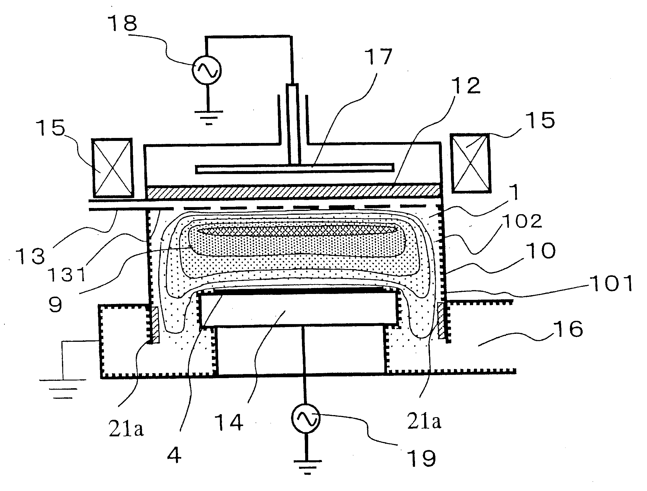
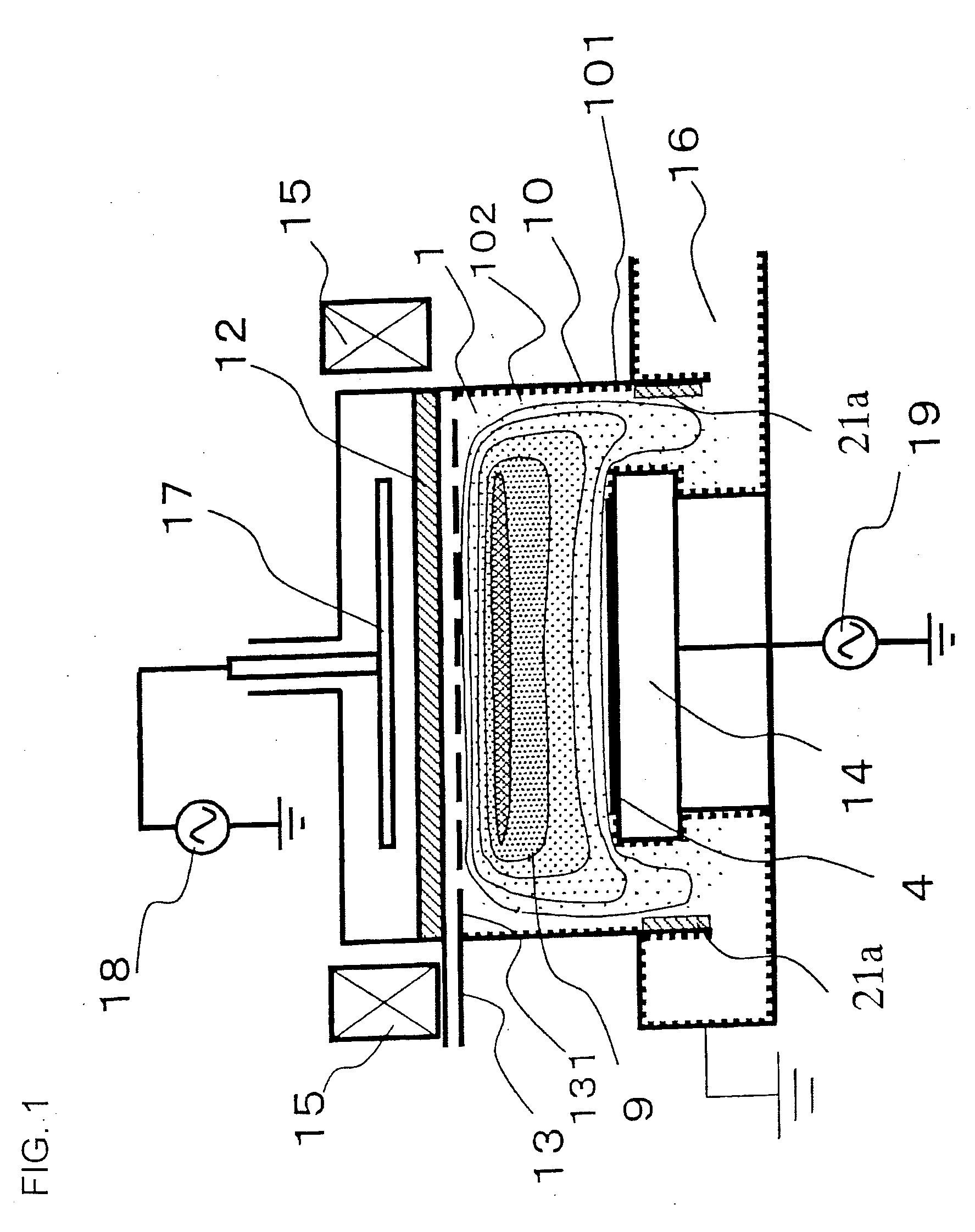
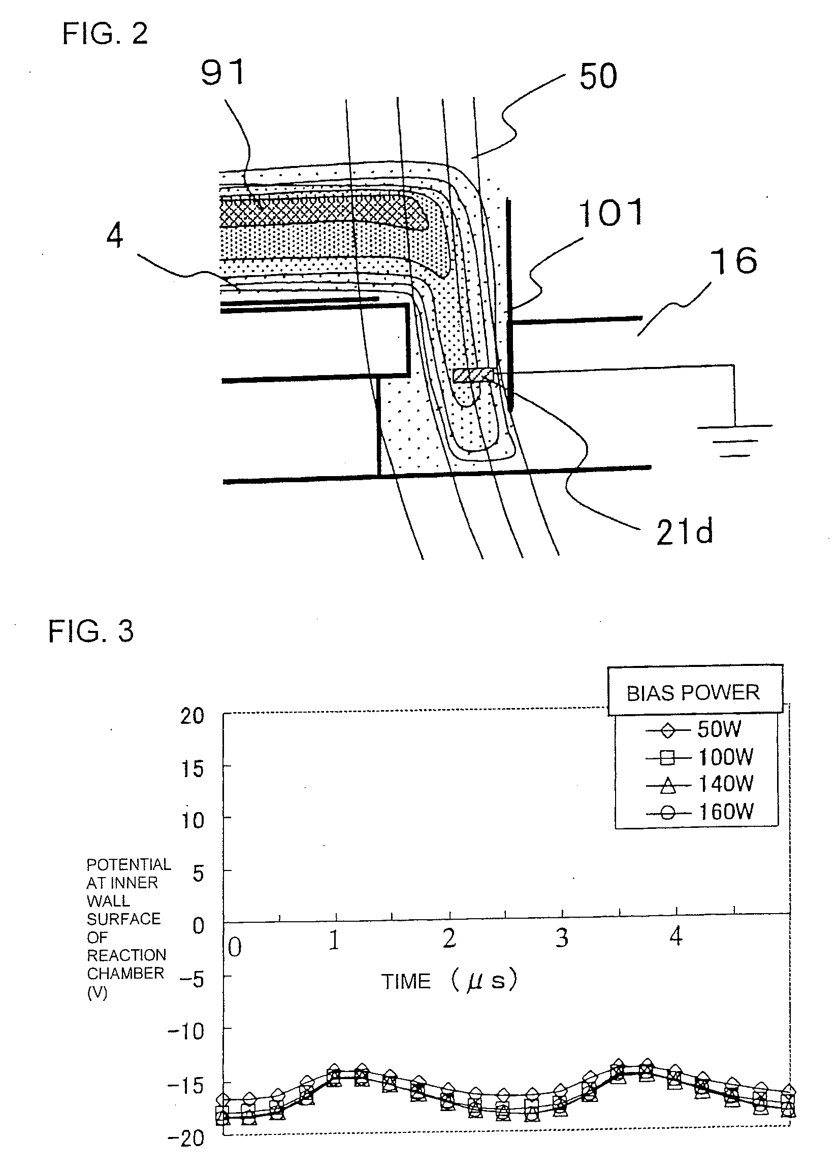
[0040] We will now describe in detail a plasma etching apparatus utilizing electromagnetic waves in the UHF band, which is one example of the plasma processing apparatus according to a first preferred embodiment of the present invention with reference to FIG. 1. The plasma etching apparatus is composed of a reaction chamber container 10 defining a reaction chamber 1, a dielectric vacuum window 12, a gas discharge plate 13 having gas discharge holes 131, a wafer holding electrode 14 functioning as a substrate holder on which a wafer 4 is mounted, a field coil 15, an exhaust outlet 16 for maintaining the inside of the reaction chamber container 10 in decompressed state, a plasma-generating high-frequency electrode 17 to which high frequency is applied from a plasma-generating high-frequency power supply 18 for generating plasma 9 inside the reaction chamber, a wafer biasing high-frequency power supply 19 for supplying a biasing high-frequency power to the wafer holding electrode 14, a...


PUM

PropertyMeasurementUnit
frequencyaaaaaaaaaa
pressureaaaaaaaaaa
diameter sizeaaaaaaaaaa

Abstract

A plasma processing method for processing a substrate with plasma by applying a high frequency to a reaction chamber, and applying a second high frequency to a substrate holder includes covering at least 90% of a total surface area of an inner wall of the reaction chamber that is directly exposed to plasma with a dielectric, disposing a DC earth comprising a conductive portion that is earthed and having an area less than 10% of the inner wall of the reaction chamber, and performing plasma processing to the substrate in the reaction chamber having the DC earth located at a position where a floating potential of plasma is higher than the floating potential of plasma at the inner wall of the reaction chamber that is closest to the substrate.

Description

CROSS REFERENCE TO RELATED APPLICATION [0001] This application is a divisional application of U.S. application Ser. No. 10 / 784,275, filed Feb. 24, 2004, the contents of which are incorporated herein by reference.FIELD OF THE INVENTION [0002] The present invention relates to a plasma processing apparatus and plasma processing method that reduce the damage to the inner walls of the reaction chamber that is caused by the application of high frequencies to a substrate to be processed, and that enable stable processing to be performed for a long time. DESCRIPTION OF THE RELATED ART [0003] Along with the miniaturization and integration of semiconductor devices and with the increase in the variety of component materials used in the devices, the plasma processing apparatuses used for manufacturing the semiconductor devices are required not only to be able to perform highly accurate processes but also to enable stable quantity output and enhanced cleanness. In a plasma etching apparatus, for...

Claims


Application Information

Patent Timeline
Patent Type & Authority Applications(United States)
IPC IPC(8): H01L21/306C23F1/00C23C16/00H01L21/3065C23F4/00H01J37/32
CPCH01J37/32477C23F4/00
Inventor TETSUKA, TSUTOMUIKENAGA, KAZUYUKIONO, TETSUOYOSHIGAI, MOTOHIKOITABASHI, NAOSHI
Owner HITACHI LTD
Why Eureka
Try Eureka