
Adhesive composition, adhesive film, and method of producing semiconductor device

a technology of adhesive film and adhesive composition, which is applied in the direction of film/foil adhesives, transportation and packaging, synthetic resin layered products, etc., can solve the problems of reducing the service life of the device, the packaging (pkg) of the device suffers from inferior moisture resistance, heat resistance, thermal stress relaxation, etc., and achieves low elastic modulus, high heat resistance, and strong adhesive strength

Inactive Publication Date: 2007-08-16
SHIN ETSU CHEM IND CO LTD
View PDF4 Cites 19 Cited by
  • Summary
  • Abstract
  • Description
  • Claims
  • Application Information

AI Technical Summary

Benefits of technology

[0017]As a result of intensive investigation aimed at achieving the above object, the inventors of the present invention discovered that an adhesive composition having a melt viscosity that falls within specific ranges prior to, and following, a specific heating operation produces a cured product that exhibits excellent filling of substrates with finely patterned circuits and excellent lamination performance at low temperatures, and also has a low elastic modulus and excellent levels of adhesive strength and heat resistance, and they were thus able to complete the present invention.

Problems solved by technology

However, despite these advantages, resin-molded packages suffer from inferior levels of moisture resistance, heat resistance, thermal stress relaxation, and heat radiation.
As a result of this increase in semiconductor chip size, and the use of semiconductor devices that have structures of the same size as the chip (CSP) (which employ area array bonding and have no lead frame), or structures that employ chip layering (such as stacked CSP and SiP), the thermal shock (stress) during the packaging (PKG) of these devices is becoming a significant problem.
), which is also problematic.
Furthermore, miniaturization is also being demanded of the support substrates onto which the semiconductor chips are mounted.
The use of liquid adhesives can cause problems, including contamination of electrodes caused by liquid adhesive exuding out around the edges of the chip during chip mounting, and wire bonding problems due to chip tilt caused by uneven thickness within the adhesive layer.
Publications such as JP 3-189127 A (patent reference 1) disclose siloxane-modified polyamideimides, but the elastic modulus of such resins is still not low enough, and the adhesion of such resins to substrates is not entirely satisfactory.
JP 10-60111 A (patent reference 2) discloses the blending of a compound having two or more maleimide groups with a siloxane-modified polyamideimide, thereby improving the high-temperature properties, but the adhesive strength of this resin composition is poor.
However, although these adhesive films offer improved adhesive strength, their filling of substrates with fine surface irregularities is unsatisfactory.
As a result, small voids can develop during die attachment, and these voids can lead to peeling of the adhesive film, meaning the films tend to suffer from reliability problems.
Furthermore, if a large quantity of an inorganic filler is added in order to improve the reliability by reducing the coefficient of water absorption and the coefficient of linear expansion, then the performance of the adhesive during low-temperature lamination to semiconductor wafers at temperatures of 100° C. or lower tends to deteriorate.

Method used


Image

  • Adhesive composition, adhesive film, and method of producing semiconductor device
  • Adhesive composition, adhesive film, and method of producing semiconductor device
  • Adhesive composition, adhesive film, and method of producing semiconductor device

Examples


synthesis example 1

Synthesis of Polyimide Resin

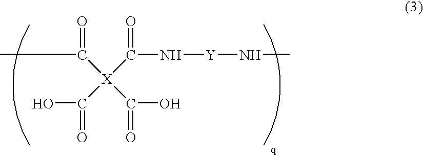
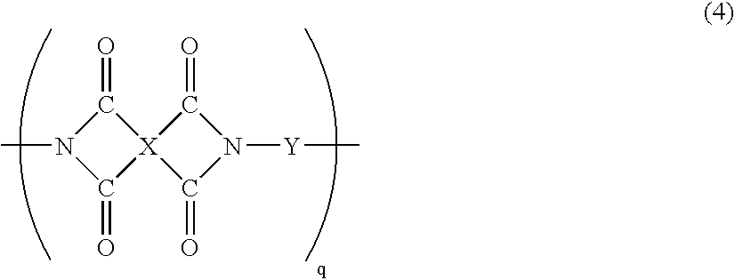
[0078]A 1 liter separable flask equipped with a 25 ml quantitative moisture receiver that is fitted with a stopcock and also connected to a reflux condenser, a thermometer, and a stirrer was charged with 44.03 parts by mass of a diaminosiloxane KF-8010 (manufactured by Shin-Etsu Chemical Co., Ltd.) represented by the structural formula shown below, and 100 parts by mass of 2-methylpyrrolidone as the reaction solvent. The mixture was stirred at 80° C., thereby dispersing the diamine. A solution containing 38.72 parts by mass of 6FDA (2,2-bis(3,4-dicarboxyphenyl)hexafluoropropane dianhydride) as the acid anhydride, and 100 parts by mass of 2-methylpyrrolidone was then added dropwise to the dispersion, and the reaction was continued under constant stirring for 2 hours at room temperature, thereby synthesizing an acid anhydride-rich amic acid oligomer.

(wherein, n=10 (average value))

[0079]Subsequently, a 1 liter separable flask equipped with a 25 ml quantitati...

examples 1 to 5

, Reference Examples 1 to 2

[0081]50 parts by mass of the polyimide resin obtained in the synthesis example 1 was dissolved in 50 parts by mass of cyclohexanone, thus forming a solution. This solution was combined with an epoxy resin RE310S (manufactured by Nippon Kayaku Co., Ltd.), dicyandiamide (DICY) (manufactured by Shikoku Chemicals Corporation) as a curing catalyst, and a 70% by mass cyclohexanone solution of silica (product name: SE2050, manufactured by Admatechs Co., Ltd.) as an inorganic filler, using the blend quantities (parts by mass) shown below in Table 1, thus yielding an adhesive composition. The properties of each of the prepared adhesive compositions were measured using the methods described below. The results of these measurements are shown in Table 1.

(1) Adhesive Composition Properties

[0082]15 μm Gap Filling Performance

[0083]Each of the resin compositions from the examples 1 to 5 and the reference examples 1 and 2 was used to form an adhesive layer (thickness: 25 ...


PUM

PropertyMeasurementUnit
Temperatureaaaaaaaaaa

Abstract

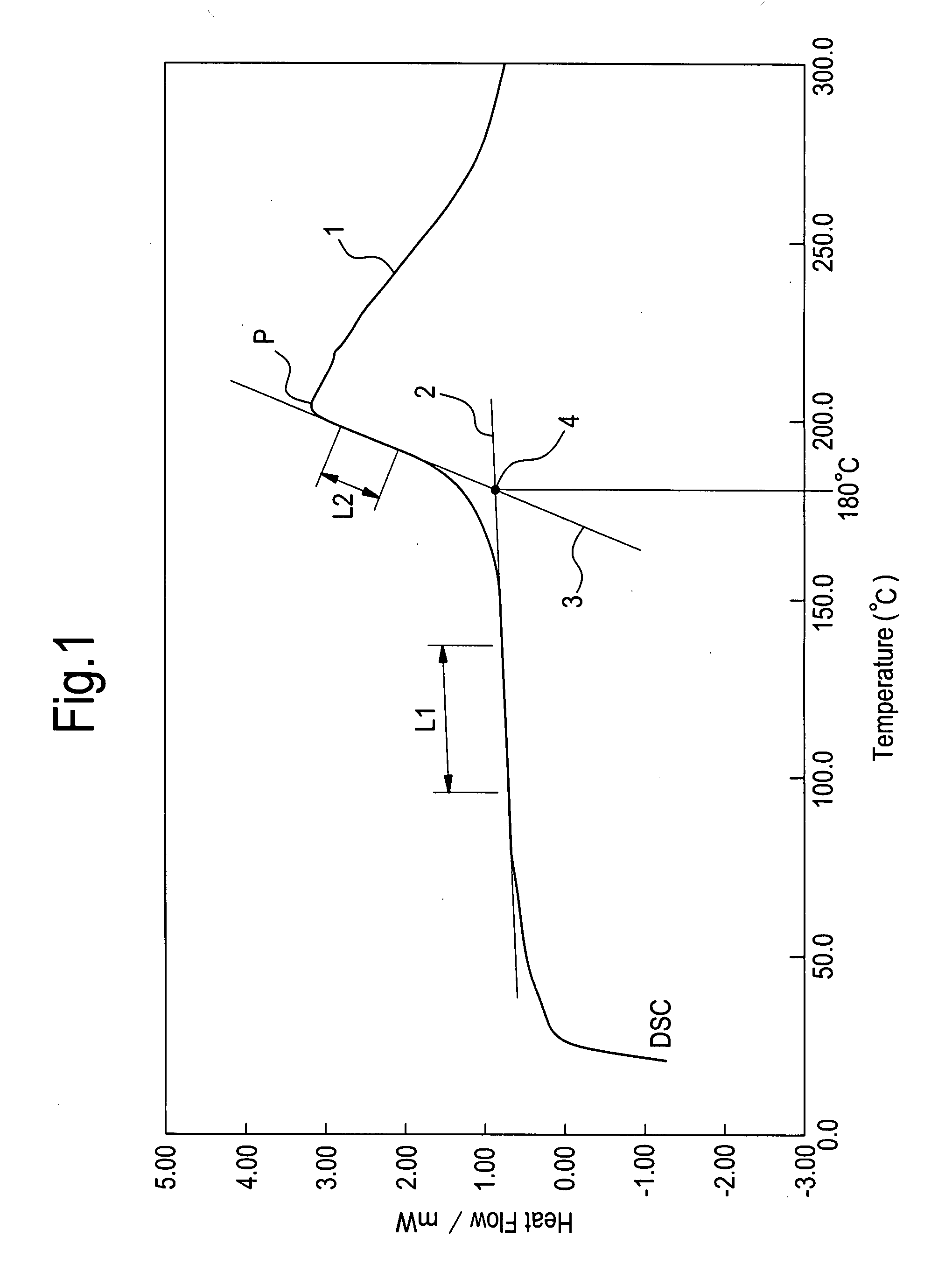
Provided is an adhesive composition, which exhibits a melt viscosity at 40 to 80° C. of not more than 10,000 Pa·s, and which after heating for a period of 1 minute to 2 hours at a temperature within a range from 80° C. to (T+50)° C., exhibits a melt viscosity at a temperature of 100° C. to (T+30)° C. that is within a range from 100 to 10,000 Pa·s (wherein, T represents the curing start temperature for the composition). The adhesive composition is capable of forming a cured product that exhibits excellent filling of substrates with finely patterned circuits, excellent lamination performance at low temperatures, a low elastic modulus, and excellent levels of adhesion and heat resistance. The adhesive composition is useful for providing an adhesive film and for producing a semiconductor device.

Description

BACKGROUND OF THE INVENTION[0001]1. Field of the Invention[0002]The present invention relates to an adhesive composition that can be used in the production of semiconductor devices, is ideal for use within resin-molded semiconductor packages, exhibits excellent filling of substrates with finely patterned surfaces, and also has a low elastic modulus and high adhesive strength, and also relates to an adhesive film that comprises such an adhesive composition, and a method of producing a semiconductor device that uses such an adhesive film.[0003]2. Description of the Prior Art[0004]In the production of a semiconductor device, a large diameter silicon wafer with IC circuits formed thereon is cut into semiconductor chips in a dicing (cutting) step, a semiconductor chip is mounted to a lead frame by thermocompression bonding or the like using a liquid adhesive (a die bonding material), wire bonding is conducted between the electrodes, and the entire structure is then sealed in order to imp...

Claims


Application Information

Patent Timeline
IPC IPC(8): C08L83/04C08L63/00C08G77/455
CPCC08L63/00C08L79/08C09J163/00C09J183/10C08L2666/22C08L2666/20C08L2666/14Y10T428/31511C09J7/00C09J2203/326
Inventor ICHIROKU, NOBUHIROKOZAKAI, SHOUHEI
Owner SHIN ETSU CHEM IND CO LTD
Learn More