Quantum interference effect transistor (QUIET)

a quantum interference and transistor technology, applied in the field of nanoscale switching devices, can solve the problems of the downscaling of the minimum geometries of the transistor-based integrated circuit will eventually be brought to an end, and the inability to meet the requirements of the system designer, so as to reduce the destructive effect of quantum interference, reduce the coherence, and reduce the effect of existing destructive quantum interferen

Inactive Publication Date: 2007-09-20
THE ARIZONA BOARD OF REGENTS ON BEHALF OF THE UNIV OF ARIZONA
View PDF2 Cites 9 Cited by
  • Summary
  • Abstract
  • Description
  • Claims
  • Application Information

AI Technical Summary

Benefits of technology

[0014] In one embodiment of the present invention, there is provided a molecular-based switching device including a molecule having first and second nodes in between which destructive quantum interference restricts electrical conduction from the first node to the second node in an off-state, a first electrode connected to the first node and configured to supply charge carriers to the first node, a second electrode connected to the second node and configured to remove charge carriers from the second node, and a control element configured to reduce coherence in or alter charge transport paths between the first and second nodes so as to reduce existing destructive quantum interference and permit flow of the charge carriers from the first node to the second node.

Problems solved by technology

In this paradigm, switching the electrical current by raising and lowering the barrier, which must have a height greater than kBT, generates a commensurate amount of heat, thereby necessitating incredible power dissipation at device densities approaching the atomic limit.
Continued downscaling steadily improves the available functionalities and pricing, while steadily challenging system designers.
However, it is expected that the downscaling of minimum geometries of transistor-based integrated circuits will eventually be brought to an end by a combination of problems related to devices, interconnections, noise, and reliability.
These problems include power dissipation, limitations in lithographic printing, thermal stability, dopant diffusion lengths, punch-through, doping levels, electric fields, and hot electrons to name a few.
However, such device architecture poses difficulties for future scaling.
One difficulty is lateral isolation of devices from each other.
Another difficulty is leakage current scaling.
Another difficulty is the diffusivity of carriers within the substrate, as free carriers (generated, e.g., by an alpha particle hit) can diffuse over many tens of microns and neutralize a stored charge.
However, many proposed solid state device implementations at this level suffer from a number of problems.
For example, critical dimensional control for devices that operate by tunneling is a problem since a barrier (e.g., a heterostructure, oxide, or otherwise) is a prerequisite for isolation in a 3-terminal device that can exhibit gain, and dimensional variations result in decidedly different device performance.
Moreover, electron tunneling is exponentially sensitive to atomic-layer fluctuations in the tunneling barriers, resulting in device characteristic variations unacceptable for large scale integration.
Meanwhile, device embodiments utilizing discrete electron charging (single-electron transistors, or SETs) suffer from reduced operating temperatures; for room temperature operation, 1 nm or less size junctions are required, dimensions which imply severe tunnel barrier fluctuation problems for solid state embodiments.
However, for nanoscale devices such as single molecules, this is impractical due to the enormous magnetic fields required to produce a phase shift of order 1 radian.
Similarly, a device based on an electrostatic phase shift would require, for the small molecules being considered, voltages incompatible with structural stability.
Thus, prior work directed to miniaturizing switching devices to the molecular dimension has been frustrated by a suitable means to control and / or modulate current flow through the nano-sized medium.

Method used


Image

  • Quantum interference effect transistor (QUIET)
  • Quantum interference effect transistor (QUIET)
  • Quantum interference effect transistor (QUIET)

Examples


example 1

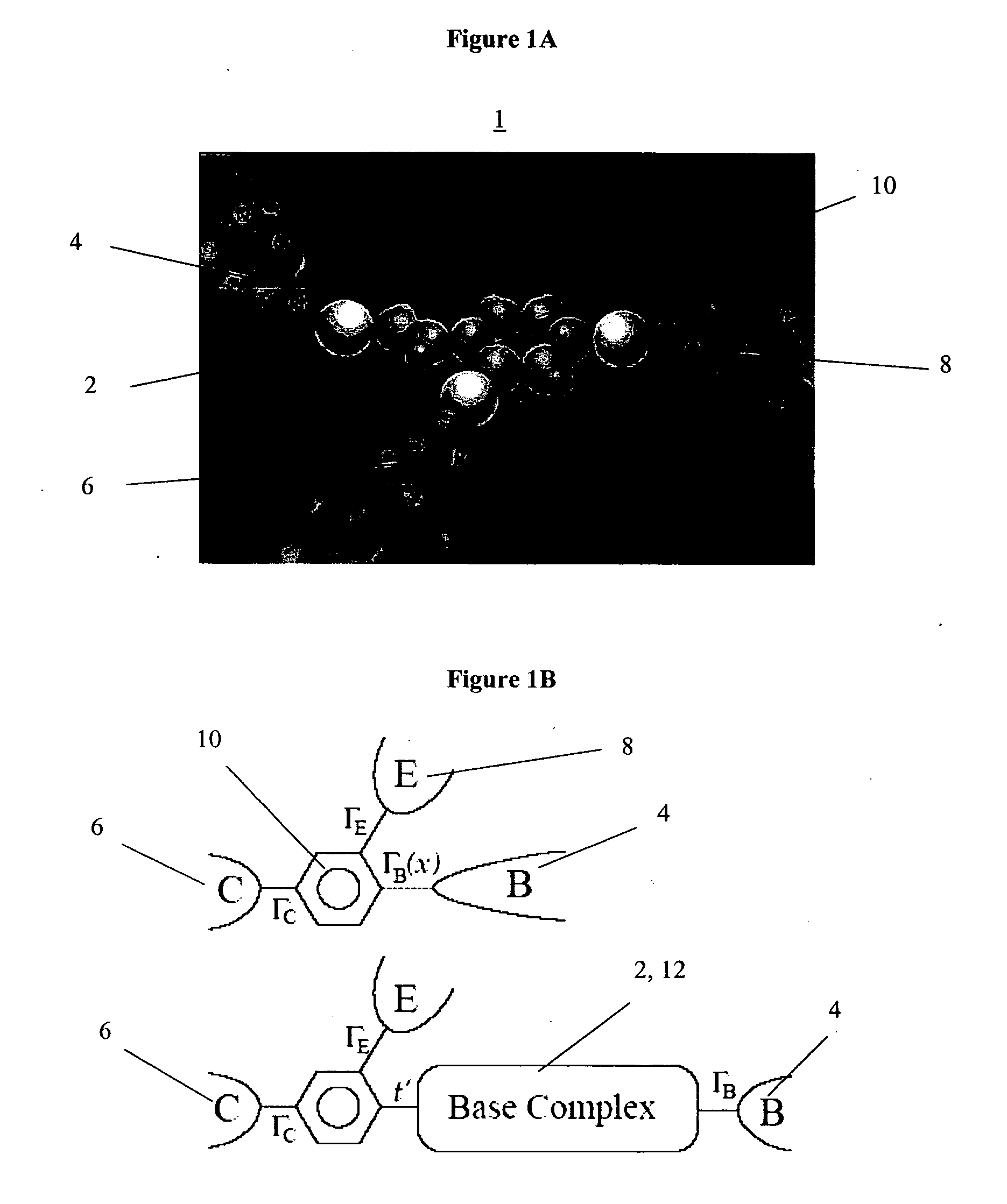
[0082] In one embodiment of the present invention, an aromatic molecule is functionalized with “alligator clips” as indicated in FIG. 10, which chemically bind to the source and drain electrodes, which are composed of appropriate metals or semiconductors, and patterned on an insulating substrate, with a separation matched to the molecular geometry. The device is fabricated by self-assembly, as described above. In this configuration, destructive quantum interference blocks the flow of electrons from the source to the drain electrode in the “off-state” of the device. The device may be “switched on” by bringing a conducting body, such as a scanning tunneling microscope tip, into close proximity (within several Angtroms) of the molecule, as illustrated schematically in FIG. 1B. The tunneling interaction of the metal tip with the electronic states of the molecule introduces decoherence, which lifts the destructive interference, and allows current to flow between the source and drain elec...

example 2

[0083] In one embodiment of the present invention, a molecule having an aromatic ring (such as benzene, [14]-annulene, [18]-annulene, or divalent metal phthalocyanine) with a side group (such as a vinyl linkage, an alkene chain, or another polymer tailored to the specific application) is synthesized with “alligator clips” at the appropriate locations on the ring for contact to the source and drain electrodes, as illustrated in FIG. 10. The alligator clips chemically bind to the source and drain electrodes, which are composed of appropriate metals or semiconductors, and are patterned on an insulating substrate, with a separation matched to the molecular geometry. The device is fabricated by self-assembly, as described above.

[0084] In this configuration, destructive quantum interference blocks the flow of electrons from the source to the drain electrode in the “off-state” of the device, when the sidegroup is not activated. The device may be switched on by “activating” the sidegroup, ...

example 3

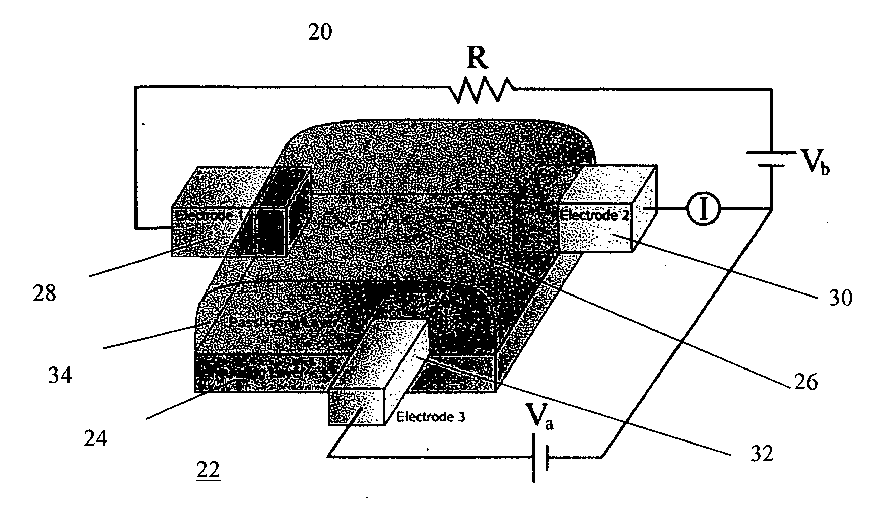
[0086] In one embodiment of the present invention, a molecule having an aromatic ring (such as for example benzene, [14]-annulene, [18]-annulene, or divalent metal phthalocyanine) with a side group (such as for example a vinyl linkage, an alkene chain, or another polymeric semiconductor) is synthesized with “alligator clips” at the appropriate locations on the ring for contact to the source and drain electrodes, as illustrated in FIG. 10, and at the end or other point of the sidegroup, for attachment to the gate electrode. The source, drain, and gate electrodes are patterned on an insulating substrate from appropriate metallic / semiconducting materials for binding to the alligator clips, with a separation matched to the molecular geometry. The three-terminal device is fabricated by self-assembly, as described above. As one particular example of this class of devices, the molecule can be sulfonated vinylbenzene, whose attachment to metal gate, source, and drain electrodes is illustrat...


PUM


Abstract

A molecular-based switching device and method for controlling charge transport across a molecule. The molecular-based switching device includes a molecule having first and second nodes in between which destructive quantum interference restricts electrical conduction from the first node to the second node in an off-state, a first electrode connected to the first node and configured to supply charge carriers to the first node, a second electrode connected to the second node and configured to remove the charge carriers from the second node, and a control element configured to reduce coherence in or alter charge transport paths between the first and second nodes so as to reduce existing destructive quantum interference and permit flow of the charge carriers from the first node to the second node. The method applies an electric potential between the first and second electrodes, controls coherence in charge transport paths between the first and second nodes so as to maintain or reduce destructive interference between the first and second nodes of the molecule, and injects charge carriers from the first electrode into the first node and collects the charge carriers from the second node at the second electrode when the coherence is controlled to reduce destructive interference.

Description

CROSS REFERENCE TO RELATED APPLICATIONS [0001] This application is related and claims priority under 35 U.S.C. 119(e) to U.S. application Ser. No. 60 / 784,503, entitled “Quantum Interference Effect Transistor (QuIET),” filed on Mar. 20, 2006, the entire contents of which are incorporated herein by reference.STATEMENT REGARDING FEDERALLY SPONSORED RESEARCH [0002] The U.S. Government may have a paid-up license in this invention and the right in limited circumstances to require the patent owner to license others on reasonable terms as provided for by the terms of the following Federal Funding from the National Science Foundation (NSF): PHY0210750, DMR0312028, DMR0406604, and PHY0244389.BACKGROUND OF THE INVENTION [0003] 1. Field of the Invention [0004] This invention is related to nanoscale switching devices in which conduction through the switching devices is controlled by quantum effects. [0005] 2. Description of the Related Art [0006] From the vacuum tube to the modern CMOS transisto...

Claims


Application Information

Patent Timeline
Patent Type & Authority Applications(United States)
IPC IPC(8): H01L29/06
CPCB82Y10/00Y10S977/709H01L51/0595H01L51/0504H10K10/701H10K10/43H10K10/00
Inventor STAFFORD, CHARLES ALLENCARDAMONE, DAVID MICHAELMAZUMDAR, SUMITENDRA
Owner THE ARIZONA BOARD OF REGENTS ON BEHALF OF THE UNIV OF ARIZONA
Why Eureka
Try Eureka