Circuit architecture for electro-optic modulation based on free carrier dispersion effect and the waveguide capacitor structures for such modulator circuitry using CMOS or Bi-CMOS process

a technology of free carrier dispersion and capacitor structure, applied in the direction of optical waveguide light guide, instruments, optics, etc., can solve the problems of fundamentally limited performance and conventional technique does not take advantage of monolithic integration between transistors and optical waveguides

Active Publication Date: 2007-12-20
LI BING
View PDF8 Cites 47 Cited by
  • Summary
  • Abstract
  • Description
  • Claims
  • Application Information

AI Technical Summary

Benefits of technology

[0010] In this invention, I discard this conventional design concept. The EO modulators invented in this application are actually circuits: the electrical-optical interaction occurs in the waveguide-capacitor, which is seamlessly, in one body or distributive manner, part of a modulator-circuit. In such way, many existing circuit design techniques can be used in the EO modulator design. The invention will show that the modulator based on free-carrier dispersion design is noting but a switching circuit design. This new design approach and the modulator circuits can improve the performance of the modulator to its physical limit, in both operation speed and power consumption.

Problems solved by technology

This conventional technique does not take the advantage of the monolithic integration between transistors and optical waveguides.
The performance is fundamentally limited due to the separation of the driving electronics and the optical waveguide itself.

Method used


Image

  • Circuit architecture for electro-optic modulation based on free carrier dispersion effect and the waveguide capacitor structures for such modulator circuitry using CMOS or Bi-CMOS process
  • Circuit architecture for electro-optic modulation based on free carrier dispersion effect and the waveguide capacitor structures for such modulator circuitry using CMOS or Bi-CMOS process
  • Circuit architecture for electro-optic modulation based on free carrier dispersion effect and the waveguide capacitor structures for such modulator circuitry using CMOS or Bi-CMOS process

Examples


invention embodiment 1

Edge-Triggered One-Shot Circuit Driving Charge Pump Modulator Circuit

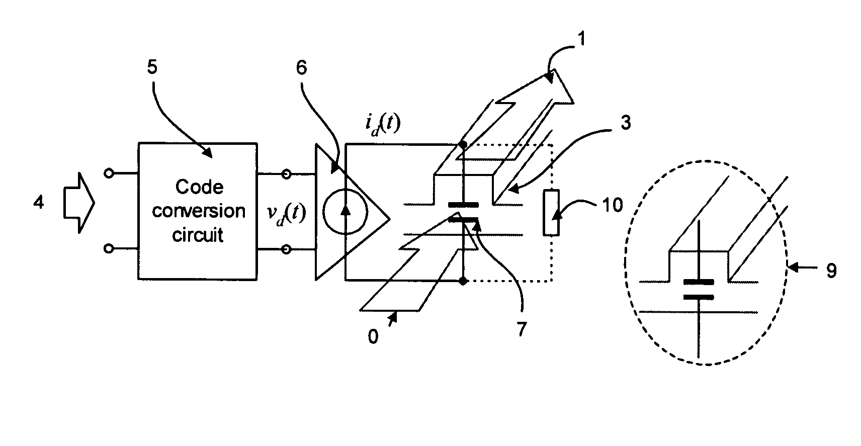
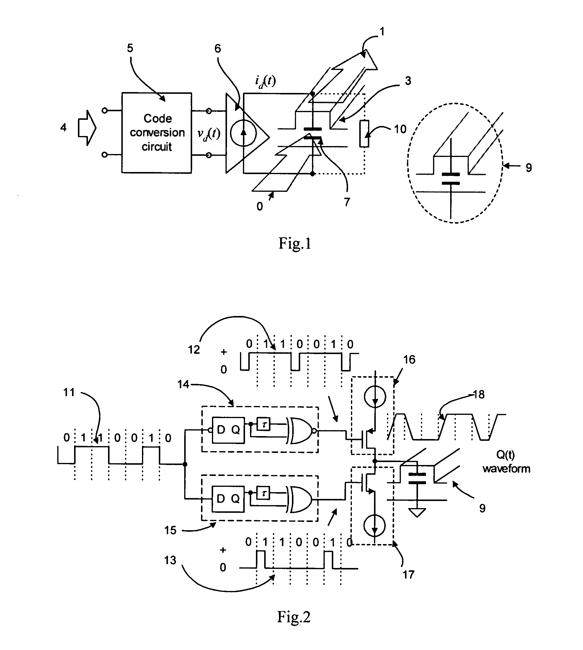
[0018]FIG. 2 gives an edge-triggered one-shot circuit driving charge pump modulation circuit, in the figure:

11>: the input electrical data, which is a non-return-zero (NRZ) code;

12>: the output of the code conversion, corresponding to the rising edge of the input data 11>;

13>: the output of the code conversion, corresponding to the falling edge of the input data 11>;

14>: rising edge triggered one-shot circuit, which generates 12>;

15>: falling edge triggered one-shot circuit, which generates 13>;

16>: charge pump circuit to charge the waveguide capacitor of the modulation circuit;

17>: charge pump circuit to discharge the waveguide capacitor of the modulation circuit;

18>: the waveform of the charge accumulated in the waveguide capacitor Q(t);

[0019] If the waveguide capacitor uses the majority carrier of the semiconductor, the self-discharge path can be ignored; the equation (1) can be simplified to: ⅆQⅆt=id...

invention embodiment 2

Low Power-Consuming Electro-Optical Modulator Circuit Using Resonator Switching

[0020] Since changing the refraction index of silicon is realized by manipulating the carrier density (either majority carrier density or minority carrier density), driving the modulator is actually charging or discharging the semiconductor junction capacitor or other capacitance structure in semiconductor (for example, MOS capacitor). In traveling wave devices, the electrical energy will propagate along the device and eventually dissipated at the termination end. The device invented here will allow us to re-use that energy for the following bits. Another description for this is, assuming always drive the modulator by return-to-zero (RZ) data, when the charging and discharging finished for one bit (logic 1 at that current bit), the energy released from the modulator-capacitor will be stored in somewhere else. If the following bit is also logic 1, the stored energy will be injected back to the modulator-c...

invention embodiment 3

Waveguide Capacitor for Electro-Optic Modulator Circuits

[0027] Another part of this invention is three new modulator waveguide capacitor structures. They are: (1) the I-type or Y-type of waveguide with gate capacitor (FIG. 6); (2) capsulated waveguide capacitor (FIG. 7); (3) bipolar transistor junctions (FIG. 8.

[0028] The I-type or Y-type of waveguide with MOS capacitor is shown in FIG. 6, in the figure:

61>: silicon area I;

62>: metal contact;

63>: gate oxide or other gate insulator in MOS;

64>: the optical mode illustration in the waveguide of the modulator;

65>: silicon area II;

66>: passivation oxide, also the top cladding of the optical waveguide;

67>: field oxide of the MOS transistor;

[0029] For the I-type waveguide capacitor, as shown in the left of FIG. 6, the surface is CMP to flat after the field oxide deposition or thermal growth. The silicon-II 65> is the original silicon layer of the SOI wafer, and the silicon-I can be the poly silicon deposited, or single crystal si...


PUM


Abstract

New circuit architecture for electro-optic modulator based on free-carrier dispersion effect is invented, in which the waveguide capacitor of the modulator is embed in the circuits and physically layout together with transistors, the switching of the modulator occurs in transistors, and as the result, the electro-optical modulation occurs in the waveguide capacitor. The invented modulator is not one physical device, it is actually a circuit. Several circuit design techniques are imported, leading to several new modulator circuits that have very high operation speed and very small power consumption. Several new waveguide capacitor structures are also invented that allow high efficient modulator circuits to be built.

Description

PRIOR PROVISIONAL PATENTS Appl. No. 60 / 810,684, Provisional filed on Jun. 5, 2006: lectro-optic modulator circuit based on free carrier dispersion effect and four new waveguide capacitor structures for the modulator using CMOS / BiCMOS process? (PDF attached) Appl. No. 60 / 599,750, Provisional filed on Aug. 9, 2004: igh speed compact electro-optic modulator on silicon? (PDF attached). BACKGROUND OF THE INVENTION [0001] The external high-speed electro-optic modulator is a necessary device for varieties of optical communication systems, where the direct modulation of the laser is not applicable due to either operation speed limitation or the frequency chirp or poor signal integrality causing unbearable impairment during the transmission. [0002] Being able to fabricate the electro-optic modulator on silicon using standard VLSI process possesses the advantages of low-cost and easy integration with electronics. Recently, extensive efforts of developing electro-optic modulator on silicon...

Claims


Application Information

Patent Timeline
Patent Type & Authority Applications(United States)
IPC IPC(8): G02B6/12
CPCG02F1/025G02F1/0121
Inventor LI, BING
Owner LI BING
Why Eureka
Try Eureka