Integrated circuit package and system interface

Active Publication Date: 2008-02-21
BELL SEMICON LLC
View PDF9 Cites 0 Cited by
  • Summary
  • Abstract
  • Description
  • Claims
  • Application Information

AI Technical Summary

Benefits of technology

[0016]It is another aspect of the present invention to provide for a method for enhancing the performance and extending the frequency range of integrated circuit packages and system interfaces.
[0018]The aforementioned aspects and other objectives and advantages can now be achieved as described herein. A method for enhancing the performance of Integrated Circuit packages and media interface is described, which includes a fissure to a Flip-Chip type package in order to improve the crosstalk performance of the package for both high and low frequencies. The wall of the fissure can be implemented utilizing a heat spreader layer and can be connected to any AC ground, such as VSS or VDD package planes.
[0019]The fissure can also accommodate the ingress of an optical fiber, which allows a direct interface with the transceivers. The direct optical fiber interface can permit the removal of solder balls for high speed signal traces, with their respective vias. On-chip integrated LED or similar light source transceivers can drive the high speed signal media. Selective deposition of low dielectric material can improve the frequency response of high speed signal package traces.
[0020]Based on the foregoing, it can be appreciated that designing high-speed analog and digital circuits for the data-communication industry is an extremely difficult task. Today, the task is especially difficult as data rates explode well beyond 1 to 40 Gbits / s. Integrated circuits, which provide the optical-to-electronic transition for these network systems, are the most difficult components to design in a fiber-optic transceiver. These optical electronic ICs (OEICs) include the laser driver, generating the electrical current to modulate the laser, and the trans-impedance amplifier, which receives a very small current from a photodiode and must amplify it with minimal noise effects. The challenge is to accurately predict the high-speed digital-signal parasitics for these optical systems. These parasitics are evaluated in the form of jitter, crosstalk, skew and ground bounce, which are generated by series inductance on the data path, substrate coupling effects at the bulk-surface level, package structure, and board-generated effects.

Problems solved by technology

Increased device complexity can generate an explosion of new creative and disruptive technology packaging solutions and in some markets and applications packaging technology is a key differentiator when making purchasing decisions.
Historically, the weakest link was the IC transceiver, due to the speed limitation of the silicon and gallium arsenide manufacturing technology.
As the CMOS process pushes the speed envelope toward the 10 Gbps arena, other system components are subject to speed limiting hurdles.
Package enclosures, mother boards and media interface connectors are becoming the performance limits for all systems above the 10 Gbps data transmission range.
All such discontinuities result in signal attenuation and reflections and destroy the signal integrity.
Equally detrimental to the signal integrity is the cross-talk, which is due to undesirable signal coupling from the adjacent package traces 170.
The IC die size can cause additional variability of the wirebond lengths.
This is clearly unacceptable for all known data transmission standards.
For high density Flip-Chip packages, the length of parallel trace coincidence can be excessive.

Method used


Image

  • Integrated circuit package and system interface
  • Integrated circuit package and system interface
  • Integrated circuit package and system interface

Examples


Embodiment Construction

[0036]The particular values and configurations discussed in these non-limiting examples can be varied and are cited merely to illustrate at least one embodiment and are not intended to limit the scope thereof.

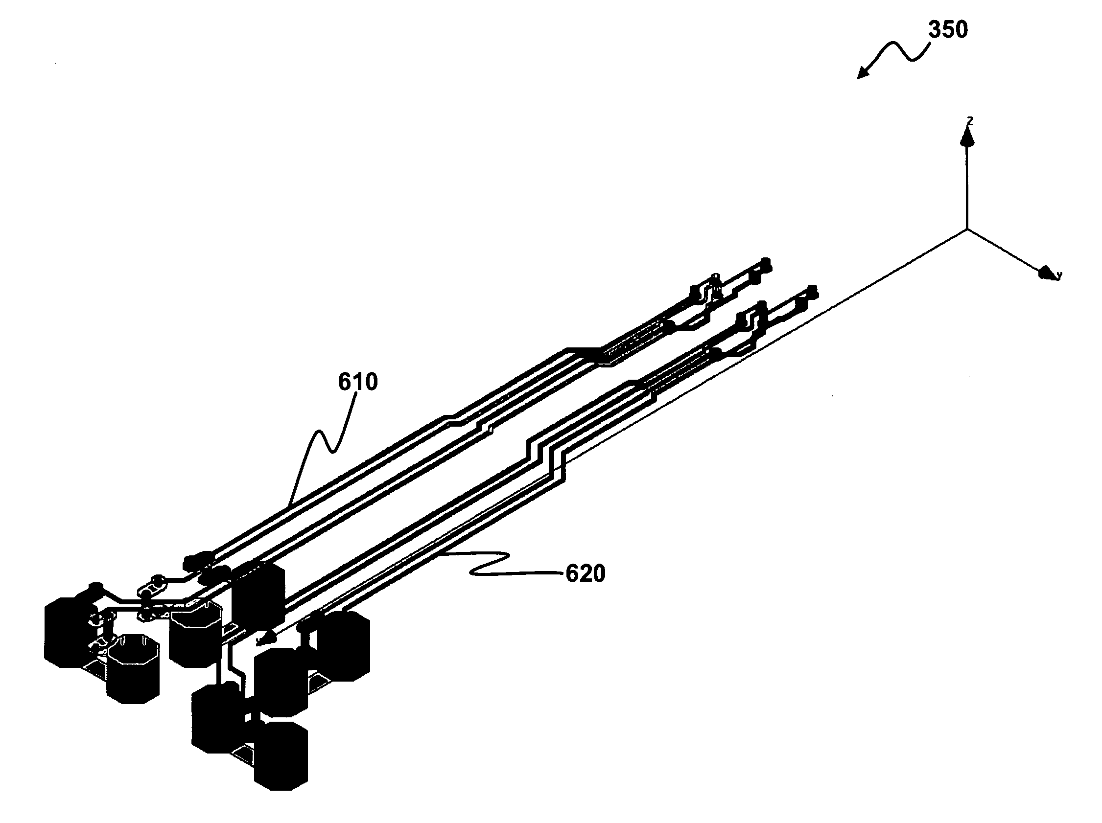
[0037]Referring to FIG. 6, a pictorial view of two signal pair traces of an integrated circuit package 350, prior to modification in accordance with a preferred embodiment. As illustrated in FIG. 6, four high-speed traces 610 form one transmit / receive pair. Adjacent four low speed signal traces 620 are analyzed for performance reference.

[0038]Referring to FIG. 7, a pictorial view of an improved IC package 400 is illustrated, in accordance with a preferred embodiment. Four high-speed traces 610 as shown in FIG. 6 are enclosed by a fissure 720. The fissure 720 is formed by conductive material 750 which are connected to VSS or VDD AC ground. The top of the fissure 720 can be formed by a conductive heat spreader 730 configured from a dielectric material 740 disposed in thermal cont...


PUM


Abstract

A method for enhancing the performance of an IC package and media interface. Adding a fissure to a Flip-Chip type package improves the crosstalk performance of the package for both high and low frequencies. The wall of the fissure can be implemented with a heat spreader layer and can be connected to any AC ground such as VSS or VDD package planes. The fissures can also accommodate the ingress of an optical fiber, which allows for a direct interface with the transceivers. The direct optical fiber interface permits the removal of solder balls for high speed signal traces, with their respective vias. On-chip integrated LEDs or other similar light source transceivers can drive the high speed signal media. Selective deposition of low dielectric material can also improve the frequency response of high speed signal package traces.

Description

TECHNICAL FIELD[0001]Embodiments are generally related to data transmission devices and systems. Embodiments are also related to Integrated Circuit (IC) packages and system interfaces. Embodiments are additionally related to methods for enhancing the performance and to extend the frequency range of IC packages and system interfaces.BACKGROUND OF THE INVENTION[0002]Consumer demand for increased mobility, wireless connectivity and advanced features have paved the way for a variety of new products including advanced mobile handsets, PDAs (Personal Digital Assistants), digital cameras and camcorders, portable music players and many other such devices. Silicon-based solutions driving these products are more highly integrated than ever before, as advancements in process technology have resulting in the delivery of System-on-a-Chip (SoC) solutions that are smaller, faster and increasingly inexpensive. These trends, along with a broad range of emerging end equipment, require a large diversi...

Claims


Application Information

Patent Timeline
IPC IPC(8): H01L23/48
CPCH01L23/66H01L24/17H01L25/165H01L2223/6627H01L2224/16H01L2924/12041H01L2924/12043H01L2924/14H01L2924/15173H01L2924/1903H01L2924/3011H01L2924/00
Inventor GASPARIK, FRANTISEKCALLICOTT, STEVE
Owner BELL SEMICON LLC
Why Eureka
Try Eureka