Fluorescent labeling reagent
a fluorescent and labeling technology, applied in the field of fluorescent labeling reagents, can solve the problems of destroying biomedical tissues such as cells, complication of measurement system and decrease in excitation light intensity, and expensive excitation light sources with such a shorter wavelength, and achieves stable and low-cost effects
- Summary
- Abstract
- Description
- Claims
- Application Information
AI Technical Summary
Benefits of technology
Problems solved by technology
Method used
Image
Examples
example 1
[0045]Acetic acid compound complex doped with rare earth elements was added to yttrium acetate and aluminum isopropoxide and they were mixed into 1,4-butanediol solvent. Then, the mixture was subjected to the glycothermal treatment using the autoclave, thereby obtaining a YAG (Yttrium Aluminum Garnet) crystalline particle including a fluorescent rare earth dopant.
example 2
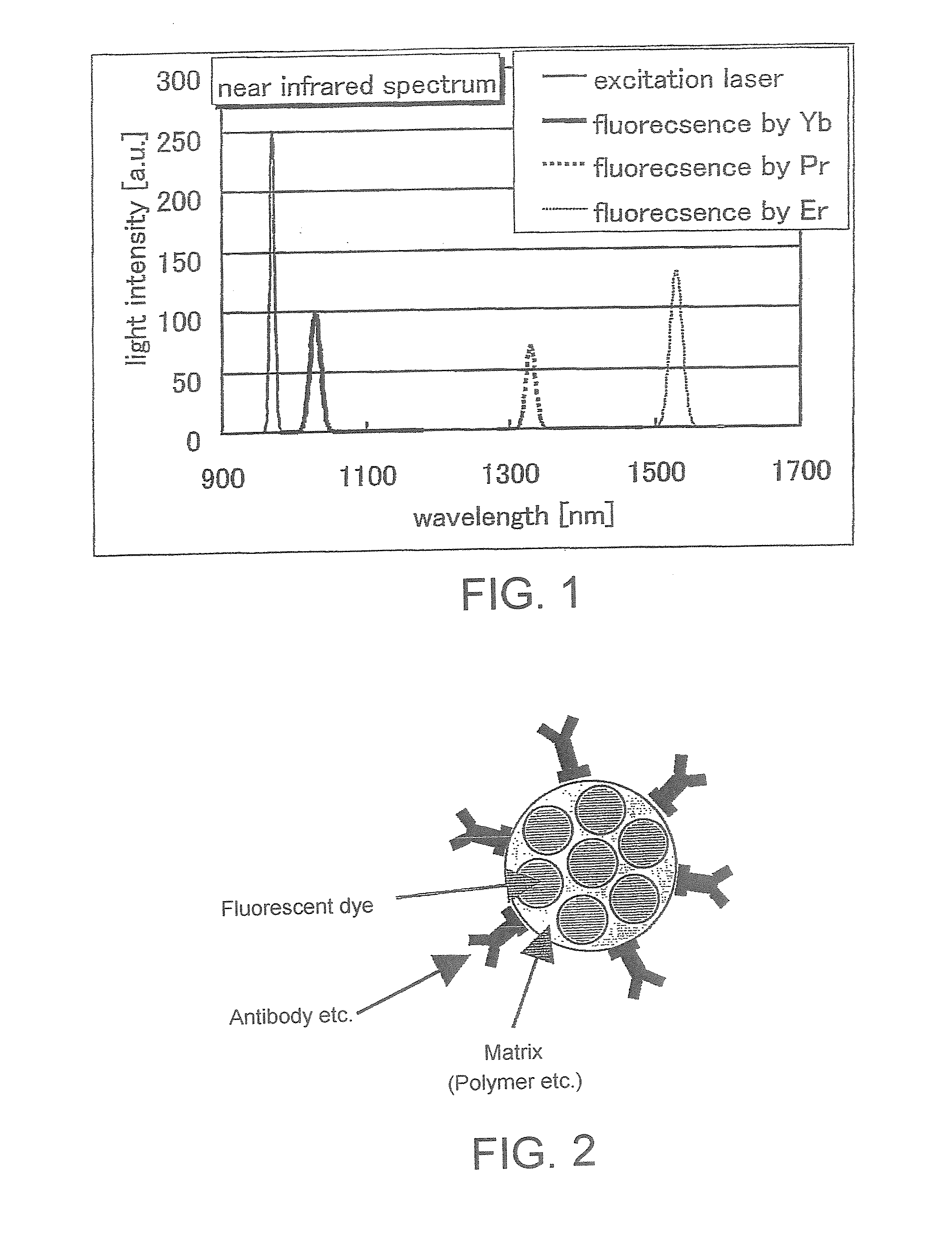
[0046]Three types of fluorescent reagents including Yb, Pr, and Er as a dopant, respectively, were simultaneously excited by an LD which radiates a laser light having the wavelength of 0.97 nm. Then, fluorescence from the respective reagents were divided into different groups of wavelengths by using a filter. The fluorescence wavelengths of the fluorescent reagents of Yb, Pr, and Er were 1.03 nm, 1.33 nm, and 1.53 nm, respectively. InGaAs or Ge photodiode or photoelectron multiplier was used as an optical detector. FIG. 1 is a graph showing spectra of the excitation laser light and the fluorescence from the respective reagents detected when performing multicoloring.
example 3
[0047]Two types of fluorescent reagents including Nd and Er as a dopant, respectively, were simultaneously excited by an LD which radiates a laser light having the wavelength 0.80 nm. Then, fluorescence from the respective reagents were divided into different groups of wavelengths by using a filter. The fluorescence wavelengths of the fluorescence reagents of Nd and Er were 1.06 nm and 1.53 nm, respectively. InGaAs or Ge photodiode or photoelectron multiplier was used as an optical detector.
PUM
| Property | Measurement | Unit |
|---|---|---|
| Diameter | aaaaa | aaaaa |
| Diameter | aaaaa | aaaaa |
| Particle size | aaaaa | aaaaa |
Abstract
Description
Claims
Application Information


