Adhesive Composition for Semiconductor Device and Cover Lay Film, Adhesive Sheet, and Copper-Clad Polymide Film Made With the Same

Inactive Publication Date: 2008-06-05
TORAY IND INC
View PDF1 Cites 12 Cited by
  • Summary
  • Abstract
  • Description
  • Claims
  • Application Information

AI Technical Summary

Benefits of technology

[0018]According to the adhesive composition of this invention, an adhesive composition for semiconductor devices which satisfies, as well as good flexural property under high temperature environment, all of high adhesive strength in room temperature, high soldering heat resistance, high flexibility and good flame retardancy can be satisfied. In addition, the adhesive sheet, the copper-clad polyimide film and the cover lay in which the adhesive composition obtained by this invention is employed are

Problems solved by technology

However, when the modulus of the adhesive layer of the composition in room temperature to 100° C. was made high, to the composition which has conventionally been investigated, in order to give a good flexural property at high temperature environment, the flexibility of FPC is damaged such that

Method used


Image

  • Adhesive Composition for Semiconductor Device and Cover Lay Film, Adhesive Sheet, and Copper-Clad Polymide Film Made With the Same
  • Adhesive Composition for Semiconductor Device and Cover Lay Film, Adhesive Sheet, and Copper-Clad Polymide Film Made With the Same
  • Adhesive Composition for Semiconductor Device and Cover Lay Film, Adhesive Sheet, and Copper-Clad Polymide Film Made With the Same

Examples


manufacturing example-1

Adhesive Sheet for Semiconductor Devices

[0069]A coating liquid in which the adhesive composition of this invention having the above-mentioned constitution is dissolved in a solvent is coated on a polyester film which is treated with a releasing agent on both sides, and the film is dried. As for the thickness of the adhesive layer, it is preferable to apply so that the thickness would be 10-100 micrometers. Drying conditions are 100-200° C. and 1-5 minutes. Although the solvent is not especially limited, aromatic type solvents such as toluene, xylene and chlorobenzene, ketone type solvents such as methyl ethyl ketone and methylethyl isobutyl ketone (MIBK), aprotic polar solvents such as dimethylformamide (DMF), dimethylacetamide and N methyl pyrrolidone, and mixtures thereof are preferable.

[0070]On the coated and dried adhesive layer, a polyester or polyolefin type protection film which has a still higher releasability is laminated, and the adhesive sheet of this invention is obtaine...

manufacturing example-2

Copper-Clad Polyimide Film

[0071]An adhesive solution is prepared by dissolving an epoxy resin, a phenoxy resin, a hardener, a hardening accelerator, an inorganic filler, a flame retarder, etc. in a solvent such as MEK (methyl ethyl ketone), MIBK (methyl isobutyl ketone), CB (chlorobenzene) or BA (benzyl alcohol). This adhesive is coated by a coater on a polyimide film (“Kapton” 100 V-P, product of Du Pont-Toray) having a thickness of 25 micrometers so that the dried thickness of the adhesive would be about 10 micrometers, dried at 150° C. for 5 minutes, and thereon, a polyester film with a silicone releasing agent having a thickness of 25 micrometers is laminated to thereby obtain an adhesive sheet. Then, the polyester film of the above-mentioned adhesive sheet is stripped, and the adhesive sheet is laminated on the dull surface of ½-oz rolled copper foil by 100° C. and 2.7 MPa and, in an air oven, heated at 150° C. for 5 hours, and a copper-clad polyimide film is produced. When pro...

manufacturing example-3

Cover Lay Film

[0072]Using the adhesives solution prepared by the same way as the above described Manufacturing example-2, this adhesive is coated by a coater on a polyimide film (“Kapton” 100 V-P, product of Du Pont-Toray) having a thickness of 25 micrometers so that the dried thickness of the adhesive would be about 30 micrometers, dried at 150° C. for 5 minutes, and thereon, a polyester film with a silicone releasing agent having a thickness of 25 micrometers is laminated to thereby obtain a cover lay film. It is common after that to adjust degree of hardening by aging at 50° C. for 20-50 hours so that the amount of bleeding of the adhesive may become proper.


PUM

PropertyMeasurementUnit
Temperatureaaaaaaaaaa
Structureaaaaaaaaaa
Flexibilityaaaaaaaaaa

Abstract

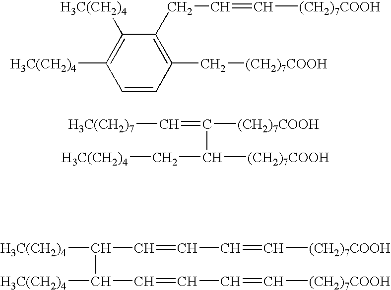
An adhesive composition for semiconductor devices which comprises an epoxy resin, a phenoxy resin, and a hardener, wherein part or all of the epoxy resin comprises at least one type of epoxy resin selected from the followings:
    • (a) a dimer acid modified epoxy resin
    • (b) a phosphorus containing epoxy resin having an epoxy equivalent of 2000 to 6000.
Said adhesive composition has satisfactory flexural properties even in a high-temperature environment while retaining an excellent toughness of the adhesive and is excellent in soldering heat resistance, adhesive property, flame retardancy and electrical properties. The adhesive composition can suitable be used for cover lay films, adhesive sheets and copper-clad polyimide films.

Description

FIELD OF THE INVENTION[0001]This invention relates to an adhesive composition for semiconductor device and cover lay film, adhesive sheet, copper-clad polyimide film made therewith.BACKGROUND ART[0002]Flexible print wiring board (hereafter referred to as FPC) is made by forming a pattern circuit by lithography, etc. on a copper-clad polyimide film (CCL) which is prepared by providing copper foil on one side or both sides of a base film represented by such as polyimide film or polyethylene terephthalate film through an adhesive layer, and by laminating thereon a cover lay film as a protective layer.[0003]This FPC is, because its thickness is usually not more than 100 micrometers and it has excellent flexibility and good flexural properties, used as various electronic equipments which have been made small and light, for example, a substrate for moving part of hard disk drive (HDD) for personal computer, a pick-up module for CD and DVD drive and a hinge substrate of cellular phone. Mor...

Claims


Application Information

Patent Timeline
IPC IPC(8): C08L63/00B32B7/10B32B7/12B32B15/08C08G59/16C08G59/30C09J7/10C09J163/00H05K1/00H05K3/28H05K3/38
CPCB32B7/12Y10T428/287B32B15/092B32B15/20B32B27/281B32B2250/03B32B2270/00B32B2307/206B32B2307/3065B32B2457/08C08G59/1472C08G59/304C09J7/00C09J163/00C09J2461/00C09J2463/00H05K1/0393H05K3/281H05K3/386Y10T428/2804Y10T428/1471B32B15/08C09J7/10C09J171/00C09J7/20C09J11/06
Inventor YAMAMOTO, TETSUYAKITAMURA, TOMOHIROSUZUKI, SACHIO
Owner TORAY IND INC
Why Eureka
Try Eureka