
Benzofluorene compound, emission materials and organic electroluminescent device

a technology of organic electroluminescent devices and emission materials, which is applied in the direction of discharge tube luminescnet screens, diaryl/triaryl methane dyes, transportation and packaging, etc., can solve the problems of device life and external quantum efficiency, luminous efficiency, current efficiency, etc., and achieve excellent solubility in solvents, excellent heat resistance, and current efficiency.

Inactive Publication Date: 2008-07-03
JNC CORP
View PDF12 Cites 47 Cited by
  • Summary
  • Abstract
  • Description
  • Claims
  • Application Information

AI Technical Summary

Benefits of technology

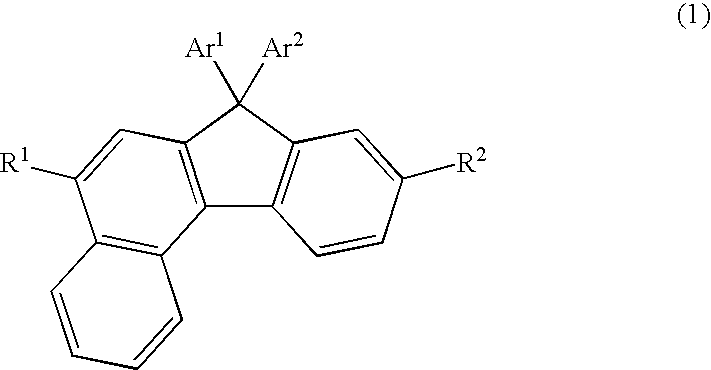
[0006]Intensive investigations repeated by the present inventors in order to solve the problems described above have resulted in successfully producing a benzofluorene compound represented by Formula (1) shown below. Further, the present inventors have found that an organic electroluminescent device which is improved in luminous efficiency, current efficiency, device life and external quantum efficiency is obtained by disposing a layer containing the benzofluorene compound between a pair of electrodes to constitute the organic electroluminescent device, and thus they have completed the present invention.
[0035]According to the preferred embodiment of the present invention, for example, a benzofluorene compound having excellent characteristics as a material for an emission layer can be provided. Also, an organic electroluminescent device which is improved in heat resistance, luminous efficiency, current efficiency, device life and external quantum efficiency can be provided. Further, the benzofluorene compound according to the preferred embodiment of the present invention is an organic material having an excellent solubility in a solvent and therefore is relatively readily synthesized, and it has the merit that it is not limited to a vapor deposition method in forming layers. As a result thereof, a material for a light emitting device which is suited to commercial production of light emitting devices can be provided.

Problems solved by technology

However, even if the organic materials described above are used, organic electroluminescent devices having satisfactory performances in terms of heat resistance, luminous efficiency, current efficiency, device life and external quantum efficiency have not yet been obtained.

Method used


Image

  • Benzofluorene compound, emission materials and organic electroluminescent device
  • Benzofluorene compound, emission materials and organic electroluminescent device
  • Benzofluorene compound, emission materials and organic electroluminescent device

Examples


example 1

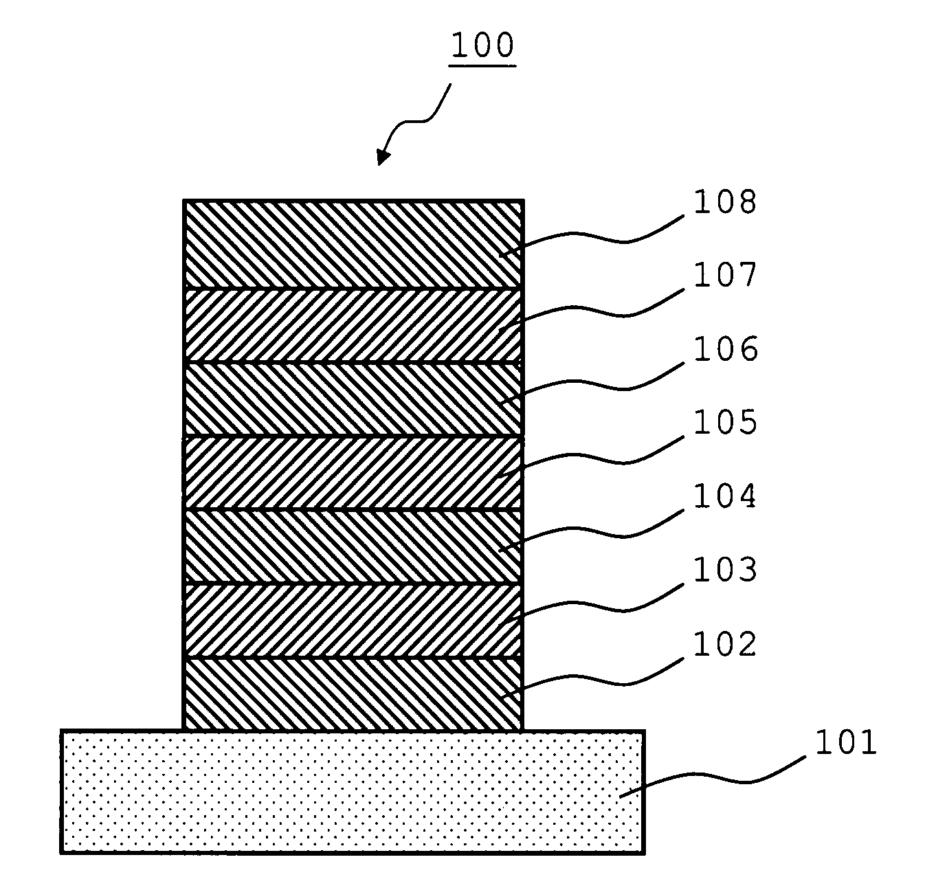
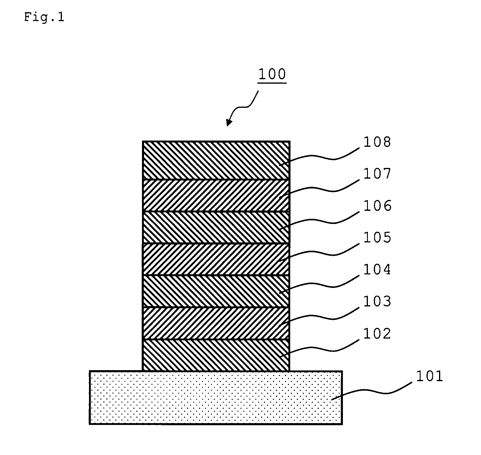
[0176]A glass substrate of 26 mm×28 mm×0.7 mm on which ITO was deposited in a thickness of 150 nm was used as a transparent substrate. This transparent substrate was fixed on a substrate holder of a commercial deposition system, and loaded therein were a molybdenum-made boat for deposition containing CuPc, a molybdenum-made boat for deposition containing NPD, a molybdenum-made boat for deposition containing the compound (1-13), a molybdenum-made boat for deposition containing D1, a molybdenum-made boat for deposition containing ALQ, a molybdenum-made boat for deposition containing lithium fluoride and a tungsten-made boat for deposition containing Aluminum.

[0177]A vacuum chamber was reduced in pressure up to 5×10⁻⁴ Pa, and the boat for deposition containing CuPc was heated to deposit it in a layer thickness of 20 nm, whereby a hole injection layer was formed. Then, the boat for deposition containing NPD was heated to deposit it in a layer thickness of 30 nm, whereby a hole transport...

example 2

[0180]An organic EL device was obtained by a method according to Example 1, except that ALQ used for the electron transport layer in Example 1 was changed to ET1. With the ITO electrode set to an anode and the lithium fluoride / aluminum electrode set to a cathode, the characteristics in emission of 100 cd / m2 were measured to find that the voltage was 3.7 V; the current density was 1.6 mA / cm2; the luminous efficiency was 5.4 μm / W; the current efficiency was 6.3 cd / A; the emission wavelength was 455 nm; and the chromaticity was (0.145, 0.168). Further, the external quantum efficiency was 4.9%, and the current density in the external quantum efficiency was 10 mA / cm2. The constant current operation test was carried out at current density for obtaining an initial luminance of 1000 cd / m2 to find that the luminance retention rate was 76.2% after 200 hours passed.

example 3

[0181]A glass substrate of 26 mm×28 mm×0.7 mm on which ITO was deposited in a thickness of 150 nm was used as a transparent substrate. This transparent substrate was fixed on a substrate holder of a commercial deposition system, and loaded therein were a molybdenum-made boat for deposition containing CuPc, a molybdenum-made boat for deposition containing NPD, a molybdenum-made boat for deposition containing the compound (1-4), a molybdenum-made boat for deposition containing D1, a molybdenum-made boat for deposition containing ALQ, a molybdenum-made boat for deposition containing lithium fluoride and a tungsten-made boat for deposition containing Aluminum.

[0182]A vacuum chamber was reduced in pressure up to 5×10⁻⁴ Pa, and the boat for deposition containing CuPc was heated to deposit it in a layer thickness of 50 nm, whereby a hole injection layer was formed. Then, the boat for deposition containing NPD was heated to deposit it in a layer thickness of 30 nm, whereby a hole transport ...


PUM

PropertyMeasurementUnit
Fractionaaaaaaaaaa
Fractionaaaaaaaaaa
Timeaaaaaaaaaa

Abstract

Provided is a benzofluorene compound which exhibits excellent performances when applied to an organic electroluminescent device.In the benzofluorene compound, a central five-membered ring in a benzofluorene skeleton is substituted with aryl, and a benzene ring condensed to the five-membered ring is substituted with aryl, diarylamino and the like.

Description

FIELD OF THE INVENTION[0001]The present invention relates to a benzofluorene compound, a material for an emission layer using the compound and an organic electroluminescent device.BACKGROUND OF THE INVENTION[0002]An organic electroluminescent device is a light emitting device which is a spontaneous emission type and is expected as a light emitting device for display or lighting. A display unit using an electroluminescent light emitting device has so far been researched in various cases because of possibility of small power consumption and reduction in a thickness. Further, an organic electroluminescent device comprising organic materials has so far been actively investigated since reduction in a weight and increase in a size are easy. In particular, developments of organic materials having light emitting characteristics including a blue color which is one of three primary colors and developments of organic materials endowed with charge transport ability (having possibility of being ...

Claims


Application Information

Patent Timeline
IPC IPC(8): C07C211/54C07C25/18H01J1/63B32B11/04C07C13/66
CPCC07C13/66H01L51/0039C07C2103/26C07C2103/40C09K11/06C09K2211/1007C09K2211/1011H01L51/0054H01L51/0058H01L51/006H01L51/0071H01L51/0072H01L51/0081H01L51/0094H05B33/14C07C2101/14C07C2601/14C07C2603/26C07C2603/40Y10T428/31504H10K85/622H10K85/626H10K85/633H10K85/6572H10K85/657H10K85/324H10K85/40C07C13/62H10K50/00H10K85/115
Inventor WANG, GUOFANGKAGEYAMA, AKIKOKOIKE, TOSHIHIROUCHIDA, MANABU
Owner JNC CORP
Learn More