HIGH EFFICIENCY PARTIAL DISTRIBUTED FEEDBACK (p-DFB) LASER

a semiconductor laser and partial distributed feedback technology, applied in the direction of lasers, semiconductor lasers, optical resonator shape and construction, etc., can solve the problems of poor power conversion efficiency of second-order dfb lasers, less attractive diode lasers as pump sources for these applications, and additional optical power loss incurred compared to fp or the first-order dfb, etc., to achieve the effect of increasing the efficiency of composite lasers

Active Publication Date: 2008-08-28
DAYLIGHT SOLUTIONS
View PDF22 Cites 4 Cited by
  • Summary
  • Abstract
  • Description
  • Claims
  • Application Information

AI Technical Summary

Benefits of technology

[0016]In still other embodiments, the invention comprises a composite laser having more than one semiconductor laser wherein at least one semiconductor laser has a partial grating and wherein the partial grating results in increased efficiency of the composite laser.

Problems solved by technology

As a result, either expensive thermal stabilization measures or very sensitive external wavelength-locking methods such as use of diffraction gratings, Fiber Bragg Gratings (FBG) or Volume Bragg Gratings (VBG) in an external cavity configuration have to be employed making diode lasers less attractive as pump sources for these applications to pump at the narrow gain band region.
However, when a second-order distributed feedback laser is fabricated there is an additional optical power loss incurred compared to a FP or the first-order DFB laser.
This problem arises because the second-order grating has a first-order diffraction that scatters light out in directions that are normal to the propagation direction of the fundamental mode.
As a result, the differential quantum efficiency (DQE) is usually lower than that for the FP or the first-order DFB laser making the power-conversion efficiency of a second-order DFB laser poorer.
This technique pertains to minimization of the transverse optical field only and does not address the issue of continual diffraction loss which occurs during propagation along the longitudinal direction as the laser light oscillates back and forth numerous times inside the DFB laser cavity.
As a result, there are no possible diffraction orders that could lead to radiation loss from the cavity modes.
However, making a first-order grating can be impractical and expensive, especially for short wavelength radiation.
While this method stabilizes the wavelength and narrows the emission bandwidth, the second-order grating distributed across the entire laser cavity leads to continuous first-order diffraction loss of radiation out of the cavity as the laser modes oscillate back and forth inside the resonator.
This technique has an additional disadvantage.
The DBR section is not electrically pumped; hence, the gain section underneath the DBR acts as a saturable absorber, reducing the overall efficiency of the laser.
Additionally, the use of a saturable absorber can also lead to a deleterious effect known as self-pulsation.

Method used


Image

  • HIGH EFFICIENCY PARTIAL DISTRIBUTED FEEDBACK (p-DFB) LASER
  • HIGH EFFICIENCY PARTIAL DISTRIBUTED FEEDBACK (p-DFB) LASER
  • HIGH EFFICIENCY PARTIAL DISTRIBUTED FEEDBACK (p-DFB) LASER

Examples


example 1

Model of Partial-Length DFB

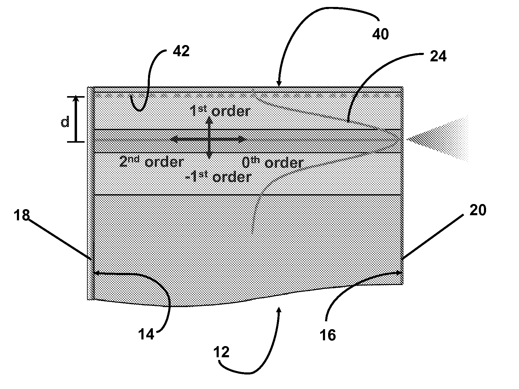
[0046]FIG. 4A shows a hypothetical example of an idealized full-length grating having a random cleave that allows the standing wave to be aligned with the peaks and valleys of the grating. This mode is strongly discriminated for by the laser because it has zero radiation loss as compared to the mode with the standing-wave peaks centered on the grating, which has maximum radiation loss. Because this hypothetical “random” cleave does not occur naturally, FIG. 4B illustrates a preferred embodiment of the invention comprising a partial grating that allows alignment of the standing wave due to its separation from the front and rear facets. This is true exactly when the right- and left-going wave intensities are the same but still has a significant effect when they are unequal.

[0047]The FP resonances have an integer number m of half-wave nodes between the facets:

mλ=2nL   (1)

where n is the index of refraction and L is the cavity length. There is a DFB region alon...

example 2

Theoretical Design

[0052]An example of one design according to an exemplary embodiment of the invention is shown in FIG. 5. If Δλ=±0.25 nm and L=2 mm then x should be between 100-400 μm and LDFB=400 μm (min. and max. are the same in this case). The value x=200 was chosen. This design is shown drawn to scale in FIG. 5.

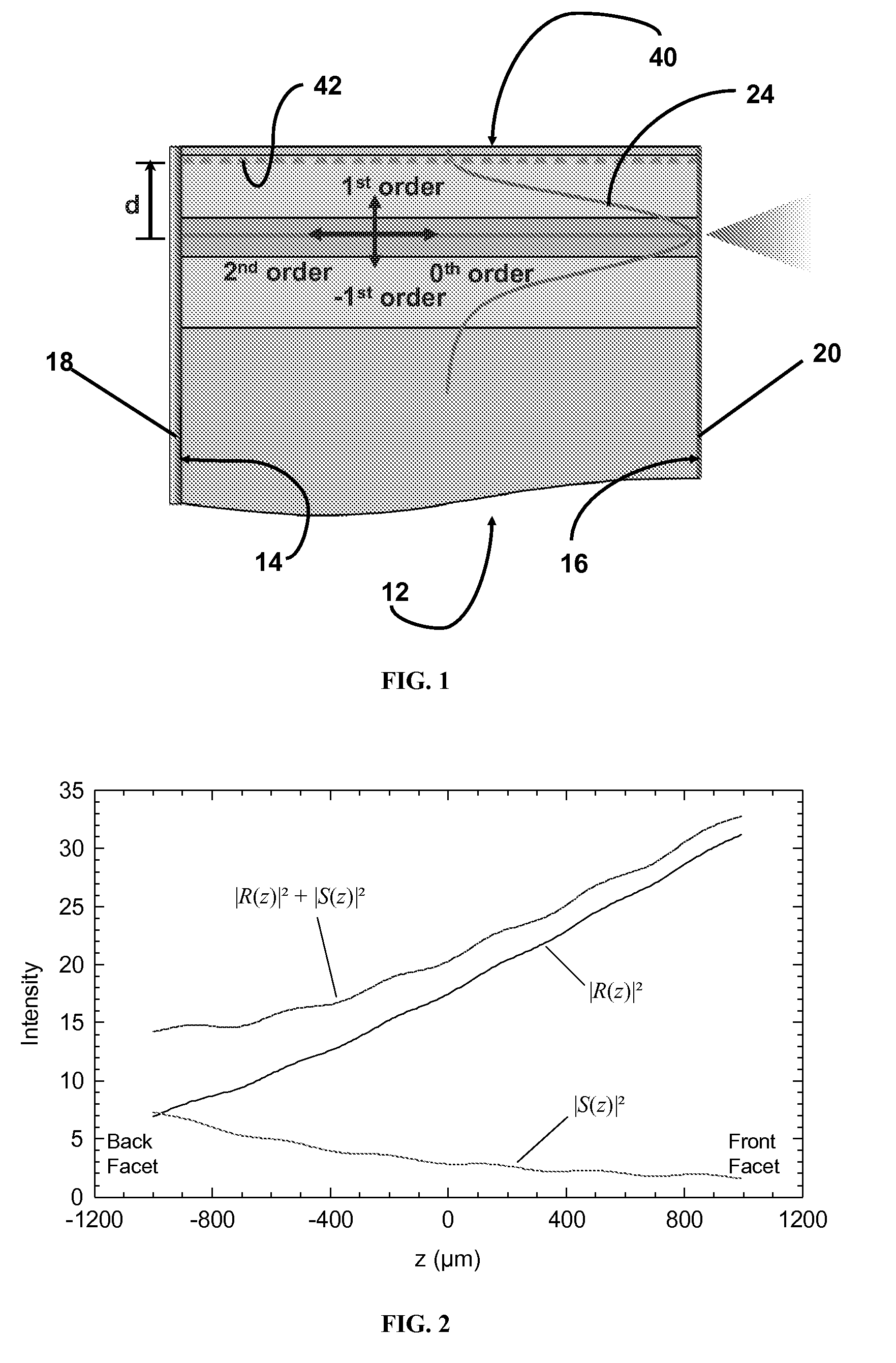
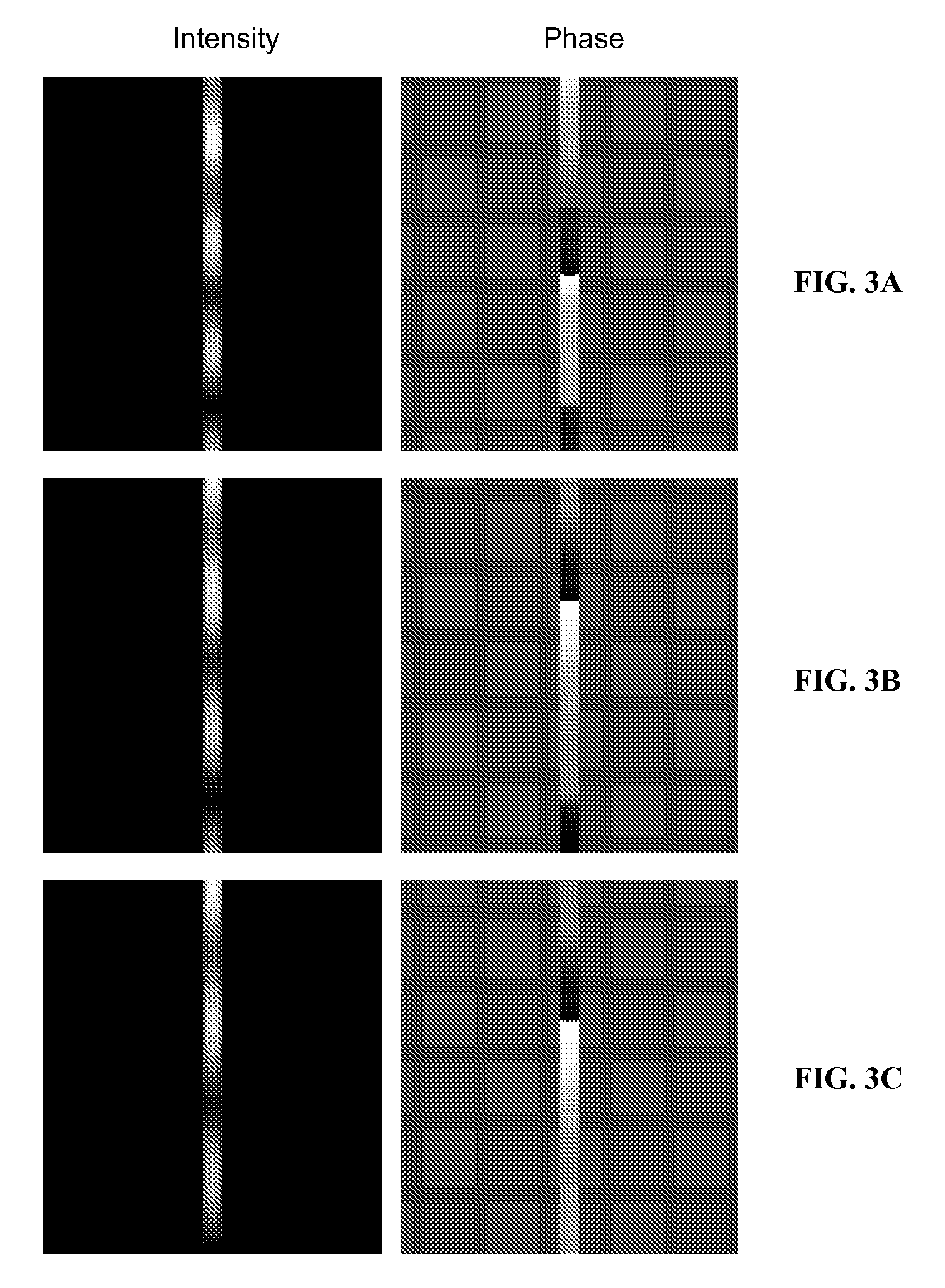
[0053]The design shown in FIG. 5 was tested using the mathematical model, above. The longitudinal field is shown in FIG. 6. The conditions were otherwise the same as those in FIG. 2 and have similar overall field profiles. Most significantly, the surface-emission power (e.g. 1st order power loss) dropped from 2.1 to 0.3 percent of the front-facet power—a factor of seven. Several different facet-cleave phases were tried and the results were similar in each case. FIG. 7 shows a typical near field surface emission from such an embodiment where the left panel shows the phase intensity image and the right panel shows the phase image. As illustrated, both the intensity and pha...

example 3

Fabrication Of The Laser

[0054]The DFB lasers were made with a two-step epitaxial growth process. The first growth comprised epitaxy of 0.6-μm thick N-cladding and 1.1-μm thick broad-waveguide core with 3.21 and 3.39 index of refraction, respectively, terminated with 0.2-μm thick InGaP layer of 3.21 index of refraction, which subsequently serves as the bottom portion of the grating layer. Second-order gratings 100-nm deep were fabricated in this layer using holographically exposed photoresist patterning and subsequent transfer of these grating patterns onto the underlying cladding layer was accomplished using reactive ion etching (RIE) technique. The second order grating has a pitch of Λ=λ / neff=0.290 μm, where λ=0.975 μm is the vacuum wavelength and neff=3.36 is the effective index of the fundamental mode in the waveguide. The remaining 0.6-μm thick P-cladding layer comprised a 0.3-μm thick (n=3.32) layer and a 0.3-μm thick (n=3.23) layer. Finally a 0.15-μm thick ps-cap GaAs layer wa...


PUM


Abstract

A second-order multi-mode partial distributed feedback (p-DFB) laser having increased electrical-to-optical power conversion efficiency, stabilized wavelength and narrowed emission linewidth. The laser includes an abbreviated grating housed in the laser cavity that is separated from both the front-end and the back-end of the laser facets.

Description

CROSS-REFERENCE TO RELATED APPLICATIONS[0001]This application seeks priority from U.S. provisional application 60 / 891,396 filed on Feb. 23, 2007, which is incorporated herein by reference in its entirety, for all purposes.FIELD OF THE INVENTION[0002]This invention pertains generally to the field of semiconductor diode lasers and particularly to edge emitting distributed feedback semiconductor lasers.BACKGROUND OF THE INVENTION[0003]Semiconductor diode lasers are formed of multiple layers of semiconductor materials. The typical semiconductor diode laser includes an n-type layer, a p-type layer and an undoped active layer between them such that when the diode is forward-biased, electrons and holes recombine in the active region layer with the resulting emission of light. The active layers (quantum well(s) resides in the waveguide layer, which has a higher index of refraction than the cladding layers that confine the emitted light to the waveguide and the active layers . Semiconductor ...

Claims


Application Information

Patent Timeline
Patent Type & Authority Applications(United States)
IPC IPC(8): H01S3/08H01L21/02H01S5/12
CPCB82Y20/00H01S5/0287H01S5/1039H01S5/34313H01S5/1203H01S5/187H01S5/12
Inventor KANSKAR, MANOJHE, YIPINGMACOMBER, STEVEN H.
Owner DAYLIGHT SOLUTIONS
Why Eureka
Try Eureka